9 mci timings – Rainbow Electronics AT91CAP9S250A User Manual
Page 981
981
6264A–CAP–21-May-07
AT91CAP9S500A/AT91CAP9S250A
47.10.9
MCI Timings
The PDC interface block controls all data routing between the external data bus, internal
MMC/SD module data bus, and internal system FIFO access through a dedicated state machine
that monitors the status of FIFO content (empty or full), FIFO address, and byte/block counters
for the MMC/SD module (inner system) and the application (user programming).
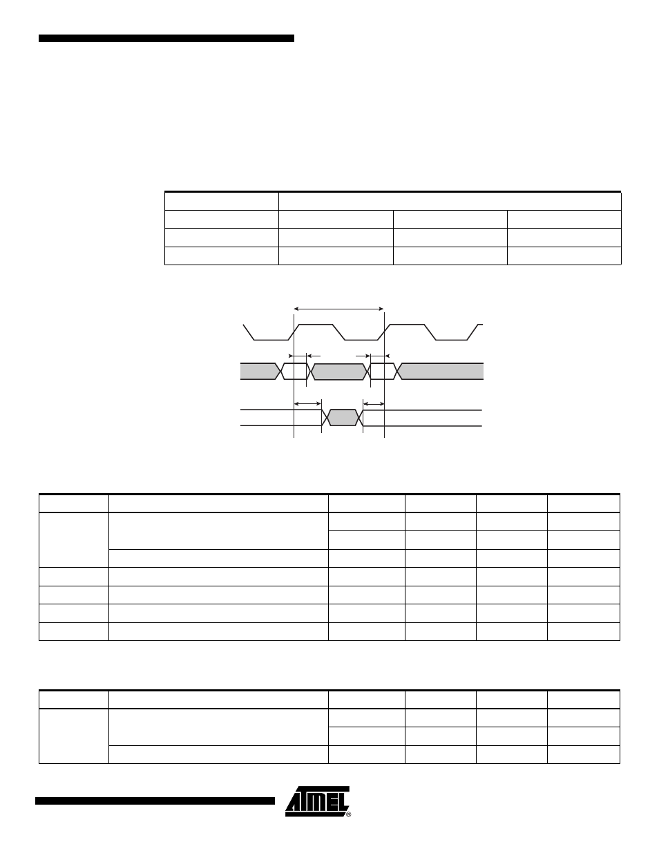
Timings are given assuming a capacitance load on data and clock.
Figure 47-12. MCI Timings
Table 47-40. Capacitance Load on Data, Clock Pads
Corner
Supply
Max
STH
Min
3.3V
25pf
25pf
25pf
1.8V
25pf
25pf
25pf
CLK
CMD_DAT Input
MCI1
CMD_DAT Output
MCI2
MCI3
MCI4
MCI5
Shaded areas are not valid
Table 47-41. MCI Timings @1.8V
Symbol
Parameter
1.8V
Min
Max
Unit
MCI
1
CLK frequency at Data transfer Mode
10 cards
25
MHz
30 cards
5
MHz
CLK frequency at Identification Mode
400
kHz
MCI
2
Input hold time
TBD
ns
MCI
3
Input setup time
TBD
ns
MCI
4
Output change after CLK rising
TBD
ns
MCI
5
Output valid before CLK rising
TBD
ns
Table 47-42. MCI Timings @3.3V
Symbol
Parameter
3.3V
Min
Max
Unit
MCI
1
CLK frequency at Data transfer Mode
10 cards
25
MHz
30 cards
5
MHz
CLK frequency at Identification Mode
400
kHz