1 pll filter, 2 divider and phase lock loop programming – Rainbow Electronics AT91CAP9S250A User Manual
Page 352
352
6264A–CAP–21-May-07
AT91CAP9S500A/AT91CAP9S250A
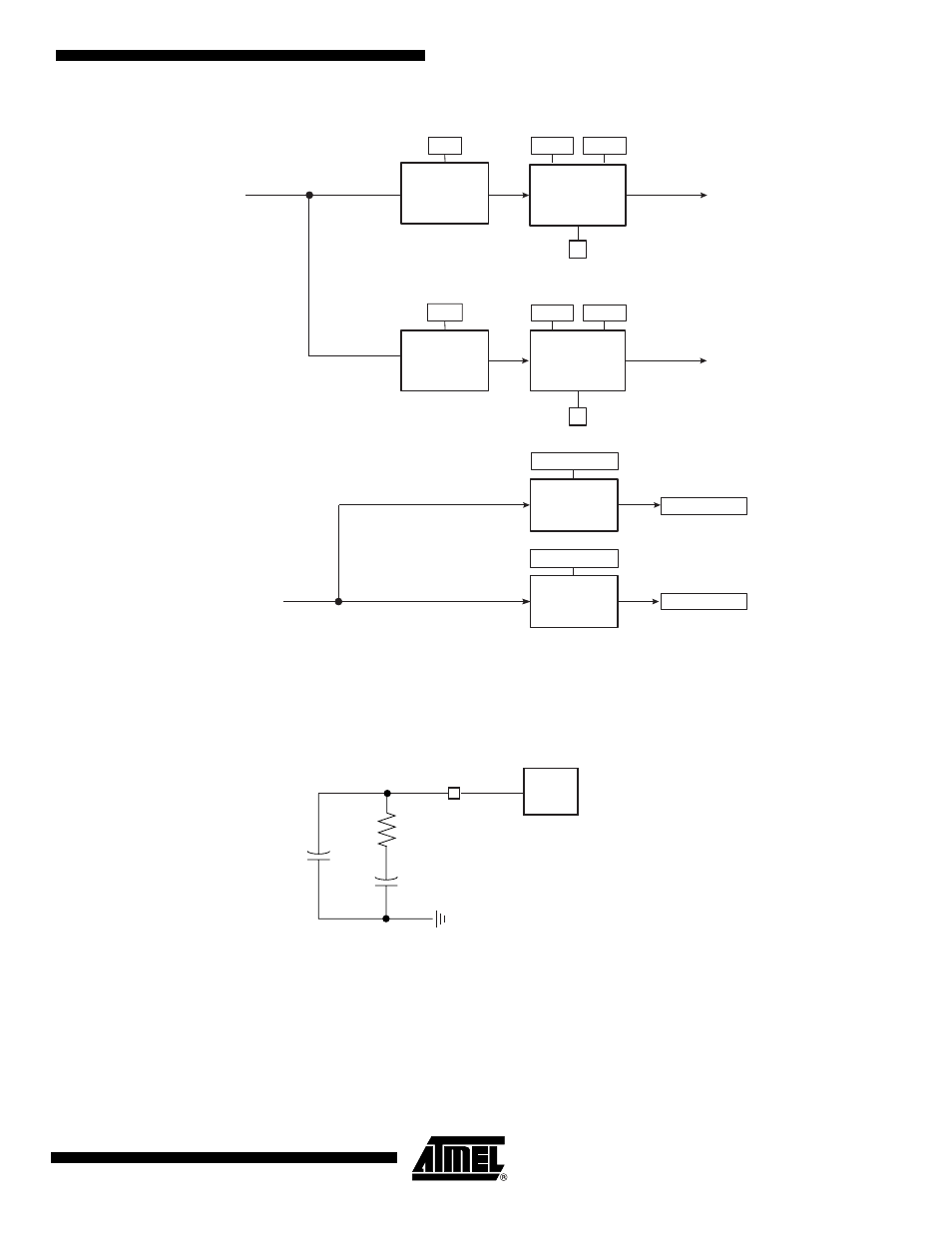
Figure 28-4. Divider and PLL Block Diagram
28.4.1
PLL Filter
The PLL requires connection to an external second-order filter through the PLLRCA and/or PLL-
RCB pin.
shows a schematic of these filters.
Figure 28-5. PLL Capacitors and Resistors
Values of R, C1 and C2 to be connected to the PLLRC pin must be calculated as a function of
the PLL input frequency, the PLL output frequency and the phase margin. A trade-off has to be
found between output signal overshoot and startup time.
28.4.2
Divider and Phase Lock Loop Programming
The divider can be set between 1 and 255 in steps of 1. When a divider field (DIV) is set to 0, the
output of the corresponding divider and the PLL output is a continuous signal at level 0. On
reset, each DIV field is set to 0, thus the corresponding PLL input clock is set to 0.
Divider B
PLLRCB
DIVB
PLL B
MULB
PLLRCA
DIVA
PLL A
Counter
PLLBCOUNT
LOCKB
PLL A
Counter
PLLACOUNT
LOCKA
MULA
OUTB
OUTA
SLCK
PLLACK
PLLBCK
Divider A
PLL B
MAINCK
GND
C1
C2
PLL
PLLRC
R