5 sdramc timings – Rainbow Electronics AT91CAP9S250A User Manual
Page 973
973
6264A–CAP–21-May-07
AT91CAP9S500A/AT91CAP9S250A
47.10.5
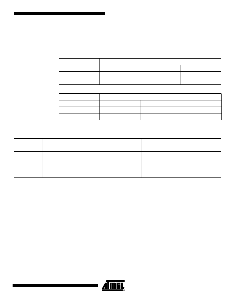
SDRAMC Timings
The SDRAM Controller satisfies the timings of standard SDRAM modules (SDRAM or mobile
SDRAM), given in
, in MAX and STH corners.
Timings are given assuming a capacitance load on data, control and address pads :
Notes:
1. Control/Address is the set of following timings : A0-A9, A11-A13, SDA10, SDCKE, SDCS, RAS, CAS, BAx, DQMx, and
SDWE
Table 47-26. Capacitance Load on Data, Control and Address Pads
Corner
Supply
MAX
STH
MIN
3.3V
50pF
50pF
0 pF
1.8V
30 pF
30 pF
0 pF
Table 47-27. Capacitance Load on SDCK Pad
Corner
Supply
MAX
STH
MIN
3.3V
10pF
10pF
10pF
1.8V
10pF
10pF
10pF
Table 47-28. SDRAMC Timings
Symbol
Parameter
Min
Units
1.8V Supply
3.3V Supply
SDRAMC
1
Control/Address/Data out valid before SDCK Rising Edge
(1)
0.5* t
CPMCK+
TBD
0.5*t
CPMCK+
TBD
ns
SDRAMC
2
Control/Address/Data out change after SDCK Rising Edge
(1)
0.5* t
CPMCK+
TBD
0.5*t
CPMCK+
TBD
ns
SDRAMC
3
Data Input Setup before SDCK Rising Edge
TBD
TBD
ns
SDRAMC
4
Data Input Hold after SDCK Rising Edge
TBD
TBD
ns