1 data timing – Rainbow Electronics AT91CAP9S250A User Manual
Page 913
913
6264A–CAP–21-May-07
AT91CAP9S500A/AT91CAP9S250A
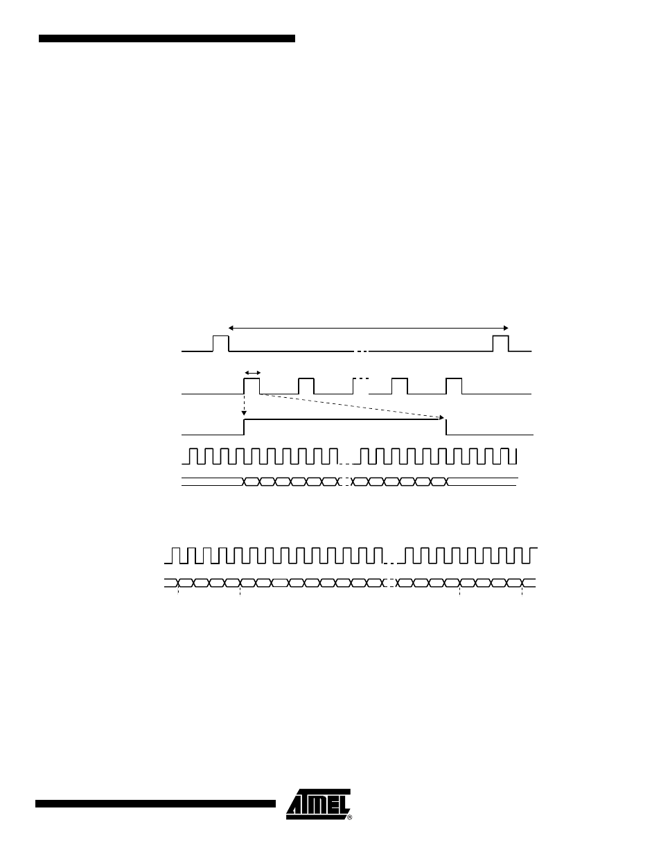
45.3.1
Data Timing
The two data timings using horizontal and vertical synchronization and EAV/SAV sequence syn-
chronization are shown in
and
.
In the VSYNC/HSYNC synchronization, the valid data is captured with the active edge of the
pixel clock (ISI_PCK), after SFD lines of vertical blanking and SLD pixel clock periods delay pro-
grammed in the control register.
The
ITU-RBT.656-4 defines the functional timing for an 8-bit wide interface.
There are two timing reference signals, one at the beginning of each video data block SAV
(0xFF000080) and one at the end of each video data block EAV(0xFF00009D). Only data sent
between EAV and SAV is captured. Horizontal blanking and vertical blanking are ignored. Use of
the SAV and EAV synchronization eliminates the ISI_VSYNC and ISI_HSYNC signals from the
interface, thereby reducing the pin count. In order to retrieve both frame and line synchronization
properly, at least one line of vertical blanking is mandatory.
Figure 45-3. HSYNC and VSYNC Synchronization
Figure 45-4. SAV and EAV Sequence Synchronization
ISI_VSYNC
ISI_HSYNC
ISI_PCK
Frame
1 line
Y
Cb
Y
Cr
Y
Cb
Y
Cr
Y
Cb
Y
Cr
DATA[7..0]
ISII_PCK
Cr
Y
Cb
Y
Cr
Y
Y
Cr
Y
Cb FF
00
DATA[7..0]
FF
00
00
80
Y
Cb
Y
00
9D
SAV
EAV
Active Video