3 application example, 1 hardware interface – Rainbow Electronics AT91CAP9S250A User Manual
Page 147
147
6264A–CAP–21-May-07
AT91CAP9S500A/AT91CAP9S250A
21.3
Application Example
21.3.1
Hardware Interface
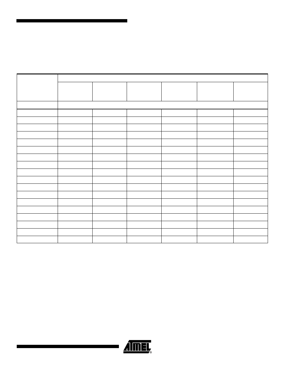
details the connections to be applied between the EBI pins and the
external devices for each Memory Controller.
Notes:
1. NWR1 enables upper byte writes. NWR0 enables lower byte writes.
2. NWRx enables corresponding byte x writes. (x = 0,1, 2 or 3)
3. NBS0 and NBS1 enable respectively lower and upper bytes of the lower 16-bit word.
4. NBS2 and NBS3 enable respectively lower and upper bytes of the upper 16-bit word.
5. BEx: Byte x Enable (x = 0,1, 2 or 3)
Table 21-2.
EBI Pins and External Static Devices Connections
Signals
Pins of the Interfaced Device
8-bit Static
Device
2 x 8-bit
Static
Devices
16-bit Static
Device
4 x 8-bit
Static
Devices
2 x 16-bit
Static
Devices
32-bit Static
Device
Controller
SMC
D0 - D7
D0 - D7
D0 - D7
D0 - D7
D0 - D7
D0 - D7
D0 - D7
D8 - D15
–
D8 - D15
D8 - D15
D8 - D15
D8 - D15
D8 - D15
D16 - D23
–
–
–
D16 - D23
D16 - D23
D16 - D23
D24 - D31
–
–
–
D24 - D31
D24 - D31
D24 - D31
A0/NBS0
A0
–
NLB
–
NLB
(3)
BE0
(5)
A1/NWR2/NBS2
A1
A0
A0
WE
(2)
NLB
(4)
BE2
(5)
A2 - A22
A[2:22]
A[1:21]
A[1:21]
A[0:20]
A[0:20]
A[0:20]
A23 - A25
A[23:25]
A[22:24]
A[22:24]
A[21:23]
A[21:23]
A[21:23]
NCS0
CS
CS
CS
CS
CS
CS
NCS1/BCCS
CS
CS
CS
CS
CS
CS
NCS2
CS
CS
CS
CS
CS
CS
NCS3/NANDCS
CS
CS
CS
CS
CS
CS
NCS4/CFCS0
CS
CS
CS
CS
CS
CS
NCS5/CFCS1
CS
CS
CS
CS
CS
CS
NRD/CFOE
OE
OE
OE
OE
OE
OE
NWR0/NWE
WE
WE
(1)
WE
WE
(2)
WE
WE
NWR1/NBS1
–
WE
(1)
NUB
WE
(2)
NUB
(3)
BE1
(5)
NWR3/NBS3
–
–
–
WE
(2)
NUB
(4)
BE3
(5)