5 8-bit nand flash, 2 gb – Rainbow Electronics AT91CAP9S250A User Manual
Page 161
161
6264A–CAP–21-May-07
AT91CAP9S500A/AT91CAP9S250A
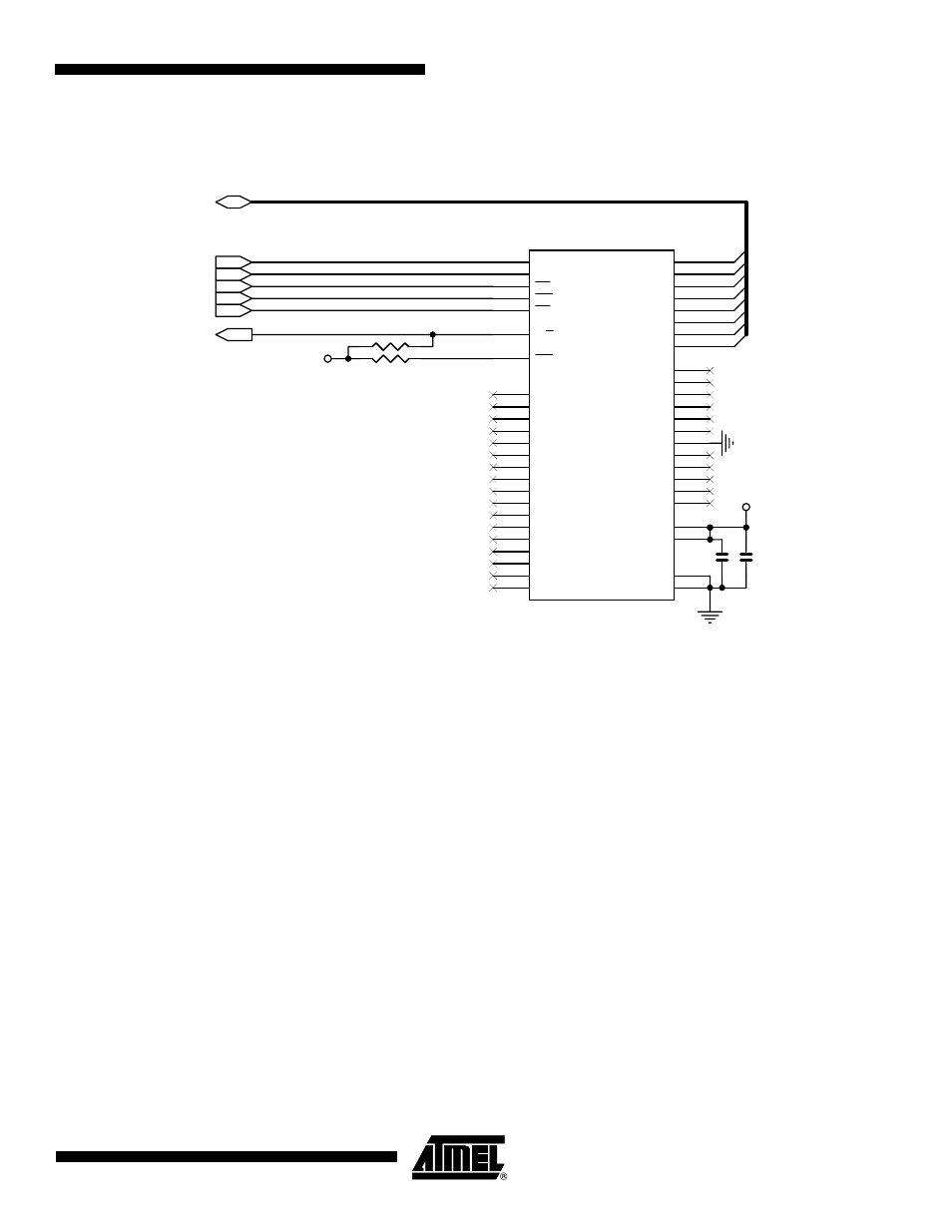
21.6.5
8-bit NAND Flash
21.6.5.1
Hardware Configuration
21.6.5.2
Software Configuration
The following configuration has to be performed:
• Assign the EBI CS3 to the NANDFlash by setting the bit EBI_CS3A in the EBI Chip Select
Assignment Register located in the bus matrix memory space
• Reserve A21 / A22 for ALE / CLE functions. Address and Command Latches are controlled
respectively by setting to 1 the address bit A21 and A22 during accesses.
• NANDOE and NANDWE signals are multiplexed with PIO lines and thus the dedicated
PIOs must be programmed in peripheral mode in the PIO controller.
• Configure a PIO line as an input to manage the Ready/Busy signal.
• Configure Static Memory Controller CS3 Setup, Pulse, Cycle and Mode accordingly to
NANDFlash timings, the data bus width and the system bus frequency.
D6
D0
D3
D4
D2
D1
D5
D7
NANDOE
NANDWE
(ANY PIO)
(ANY PIO)
ALE
CLE
D[0..7]
3V3
3V3
2 Gb
TSOP48 PACKAGE
U1
K9F2G08U0M
U1
K9F2G08U0M
WE
18
N.C
6
VCC
37
CE
9
RE
8
N.C
20
WP
19
N.C
5
N.C
1
N.C
2
N.C
3
N.C
4
N.C
21
N.C
22
N.C
23
N.C
24
R/B
7
N.C
26
N.C
27
N.C
28
I/O0
29
N.C
34
N.C
35
VSS
36
PRE
38
N.C
39
VCC
12
VSS
13
ALE
17
N.C
11
N.C
10
N.C
14
N.C
15
CLE
16
N.C
25
N.C
33
I/O1
30
I/O3
32
I/O2
31
N.C
47
N.C
46
N.C
45
I/O7
44
I/O6
43
I/O5
42
I/O4
41
N.C
40
N.C
48
R2
10K
R2
10K
C2
100NF
C2
100NF
R1
10K
R1
10K
C1
100NF
C1
100NF