2 tdf optimization enabled (tdf_mode = 1), 3 tdf optimization disabled (tdf_mode = 0) – Rainbow Electronics AT91CAP9S250A User Manual
Page 191
191
6264A–CAP–21-May-07
AT91CAP9S500A/AT91CAP9S250A
22.10.2
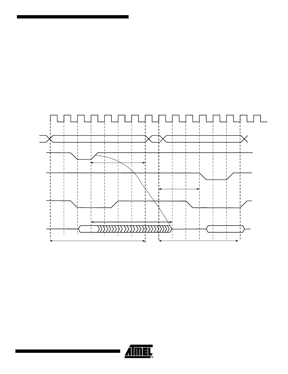
TDF Optimization Enabled (TDF_MODE = 1)
When the TDF_MODE of the SMC_MODE register is set to 1 (TDF optimization is enabled), the
SMC takes advantage of the setup period of the next access to optimize the number of wait
states cycle to insert.
shows a read access controlled by NRD, followed by a write access controlled by
NWE, on Chip Select 0. Chip Select 0 has been programmed with:
NRD_HOLD = 4; READ_MODE = 1 (NRD controlled)
NWE_SETUP = 3; WRITE_MODE = 1 (NWE controlled)
TDF_CYCLES = 6; TDF_MODE = 1 (optimization enabled).
Figure 22-22. TDF Optimization: No TDF wait states are inserted if the TDF period is over when the next access begins
22.10.3
TDF Optimization Disabled (TDF_MODE = 0)
When optimization is disabled, tdf wait states are inserted at the end of the read transfer, so that
the data float period is ended when the second access begins. If the hold period of the read1
controlling signal overlaps the data float period, no additional tdf wait states will be inserted.
illustrate the cases:
• read access followed by a read access on another chip select,
• read access followed by a write access on another chip select,
• read access followed by a write access on the same chip select,
with no TDF optimization.
A
[25:2]
NCS0
MCK
NRD
NWE
D[31:0]
Read to Write
Wait State
TDF_CYCLES = 6
read access on NCS0 (NRD controlled)
NRD_HOLD= 4
NWE_SETUP= 3
write access on NCS0 (NWE controlled)