Static memory controller (smc), 1 description, 2 i/o lines description – Rainbow Electronics AT91CAP9S250A User Manual
Page 169: 3 multiplexed signals
169
6264A–CAP–21-May-07
AT91CAP9S500A/AT91CAP9S250A
22. Static Memory Controller (SMC)
22.1
Description
The Static Memory Controller (SMC) generates the signals that control the access to the exter-
nal memory devices or peripheral devices. It has
6
Chip Selects and a 26-bit address bus. The
32-bit data bus can be configured to interface with 8-, 16-, or 32-bit external devices. Separate
read and write control signals allow for direct memory and peripheral interfacing. Read and write
signal waveforms are fully parametrizable.
The SMC can manage wait requests from external devices to extend the current access. The
SMC is provided with an automatic slow clock mode. In slow clock mode, it switches from user-
programmed waveforms to slow-rate specific waveforms on read and write signals. The SMC
supports asynchronous burst read in page mode access for page size up to 32 bytes.
22.2
I/O Lines Description
22.3
Multiplexed Signals
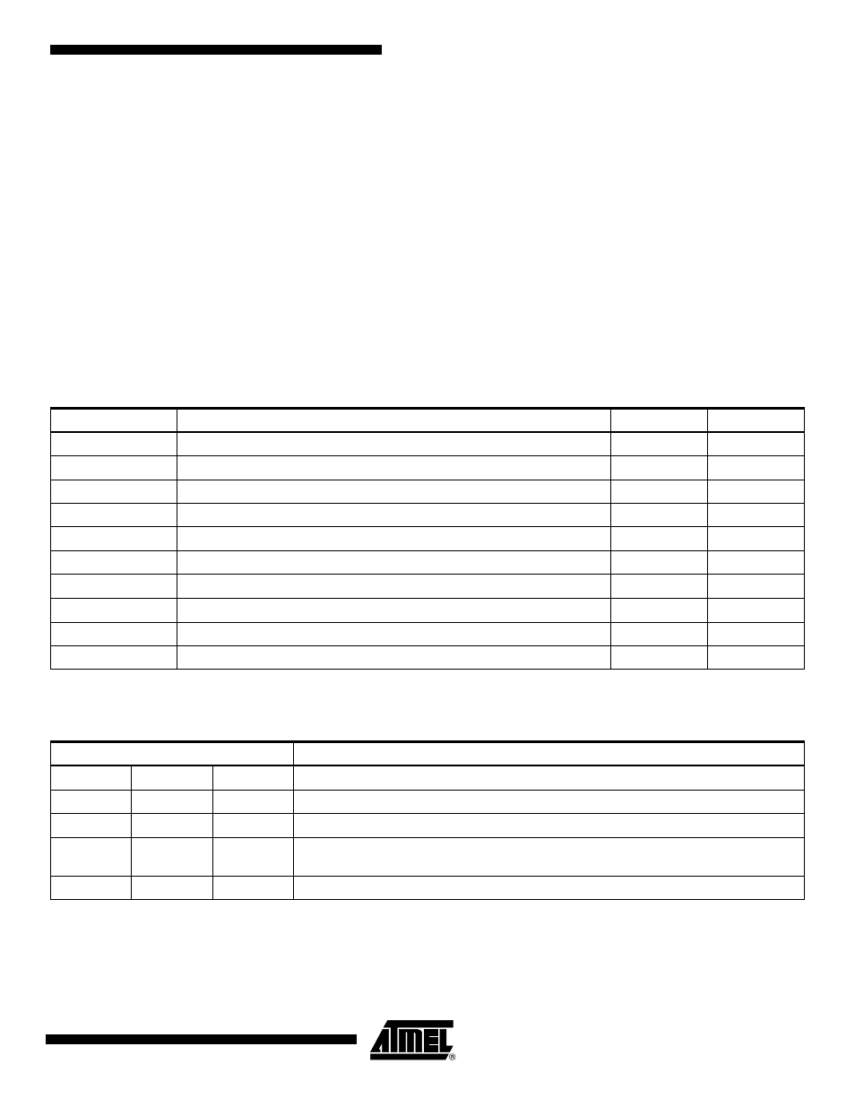
Table 22-1.
I/O Line Description
Name
Description
Type
Active Level
NCS[7:0]
Static Memory Controller Chip Select Lines
Output
Low
NRD
Read Signal
Output
Low
NWR0/NWE
Write 0/Write Enable Signal
Output
Low
A0/NBS0
Address Bit 0/Byte 0 Select Signal
Output
Low
NWR1/NBS1
Write 1/Byte 1 Select Signal
Output
Low
A1/NWR2/NBS2
Address Bit 1/Write 2/Byte 2 Select Signal
Output
Low
NWR3/NBS3
Write 3/Byte 3 Select Signal
Output
Low
A[25:2]
Address Bus
Output
D[31:0] Data
Bus
I/O
NWAIT
External Wait Signal
Input
Low
Table 22-2.
Static Memory Controller (SMC) Multiplexed Signals
Multiplexed Signals
Related Function
NWR0
NWE
Byte-write or byte-select access, see
“Byte Write or Byte Select Access” on page 171
A0
NBS0
8-bit or 16-/32-bit data bus, see
NWR1
NBS1
Byte-write or byte-select access see
“Byte Write or Byte Select Access” on page 171
A1
NWR2
NBS2
8-/16-bit or 32-bit data bus, see
.
Byte-write or byte-select access, see
“Byte Write or Byte Select Access” on page 171
NWR3
NBS3
Byte-write or byte-select access see