10 timings, 1 corner definition, 2 processor clock – Rainbow Electronics AT91CAP9S250A User Manual
Page 968: 3 maximum speed of the i/os
968
6264A–CAP–21-May-07
AT91CAP9S500A/AT91CAP9S250A
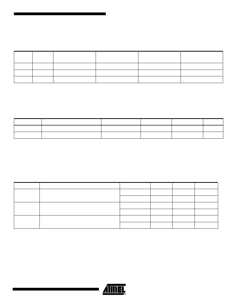
47.10 Timings
47.10.1
Corner Definition
Timings in MAX corner always result from the extraction and comparison of timings in MAX and MIN corners.
Timings in STH corner always result from the extraction and comparision of timings in STH and MIN corners.
47.10.2
Processor Clock
47.10.3
Maximum Speed of the I/Os
Criteria used to define the maximum frequency of the I/Os:
• output duty cycle (40%-60%)
• minimum output swing: 100mV to VDDIO - 100mV
• Addition of rising and falling time inferior to 75% of the period
Notes:
1. Pin Group x = To Be Defined for each product
2. 3.3V domain: V
VDDIOP
from 3.0V to 3.6V, maximum external capacitor = 40pF
3. 1.8V domain: V
VDDIOP
from 1.65V to 1.95V, maximum external capacitor = 20pF
Table 47-18. Corner Definition
Corner
Process
Temp
(External ; Junction)
VDDCORE: 1.2V
VDDIO: 1.8V
VDDIO: 3.3V
MAX
Slow
85°C ; 100°C
1.10V
1.65V
3.0V
STH
Slow
85°C; 100°C
1.2V
1.8V
3.3V
MIN
Fast
-40C; -40C
1.32V
1.95V
3.6V
Table 47-19. Processor Clock Waveform Parameters
Symbol
Parameter
Conditions
Min
Max
Units
1/(t
CPPCK
)
Processor Clock Frequency
Corner MAX
200
MHz
1/(t
CPPCK
)
Processor Clock Frequency
Corner STH
TBD
MHz
Table 47-20.
Symbol
Parameter
Conditions
Min
Max
Units
FreqMax
Pin Group x
frequency
3.3V domain
TBD
MHz
1.8V domain
TBD
MHz
PulseminH
Pin Group
High Level Pulse Width
3.3V domain
TBD
ns
1.8V domain
TBD
ns
PulseminL
Pin Group x
Low Level Pulse Width
3.3V domain
TBD
ns
1.8V domain
TBD
ns