Rainbow Electronics AT91CAP9S250A User Manual
Page 181
181
6264A–CAP–21-May-07
AT91CAP9S500A/AT91CAP9S250A
22.8.3.3
Write Cycle
The write_cycle time is defined as the total duration of the write cycle, that is, from the time
where address is set on the address bus to the point where address may change. The total write
cycle time is equal to:
NWE_CYCLE = NWE_SETUP + NWE_PULSE + NWE_HOLD
= NCS_WR_SETUP + NCS_WR_PULSE + NCS_WR_HOLD
All NWE and NCS (write) timings are defined separately for each chip select as an integer num-
ber of Master Clock cycles. To ensure that the NWE and NCS timings are coherent, the user
must define the total write cycle instead of the hold timing. This implicitly defines the NWE hold
time and NCS (write) hold times as:
NWE_HOLD = NWE_CYCLE - NWE_SETUP - NWE_PULSE
NCS_WR_HOLD = NWE_CYCLE - NCS_WR_SETUP - NCS_WR_PULSE
22.8.3.4
Null Delay Setup and Hold
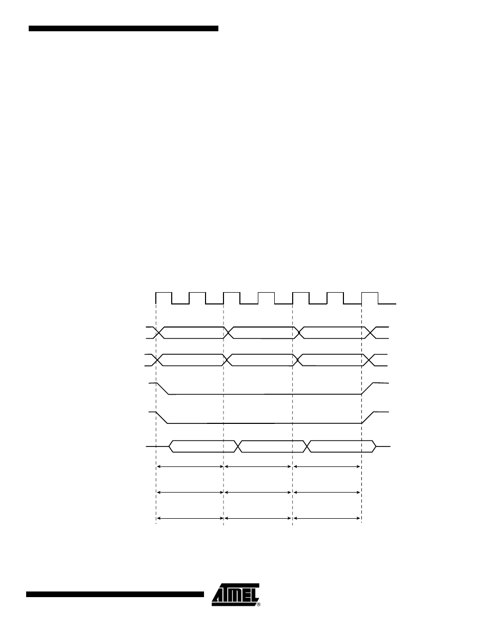
If null setup parameters are programmed for NWE and/or NCS, NWE and/or NCS remain active
continuously in case of consecutive write cycles in the same memory (see
). How-
ever, for devices that perform write operations on the rising edge of NWE or NCS, such as
SRAM, either a setup or a hold must be programmed.
Figure 22-13. Null Setup and Hold Values of NCS and NWE in Write Cycle
22.8.3.5
Null Pulse
Programming null pulse is not permitted. Pulse must be at least set to 1. A null value leads to
unpredictable behavior.
NCS
MCK
NWE,
NWR0, NWR1,
NWR2, NWR3
D[31:0]
NWE_PULSE
NCS_WR_PULSE
NWE_CYCLE
NWE_PULSE
NCS_WR_PULSE
NWE_CYCLE
NWE_PULSE
NCS_WR_PULSE
NWE_CYCLE
A
[25:2]
NBS0, NBS1,
NBS2, NBS3,
A0, A1