Table 21-5 – Rainbow Electronics AT91CAP9S250A User Manual
Page 152
152
6264A–CAP–21-May-07
AT91CAP9S500A/AT91CAP9S250A
The CFCE1 and CFCE2 waveforms are identical to the corresponding NCSx waveform. For
details on these waveforms and timings, refer to the section “Static Memory Controller”.
21.5.8.3
Read/Write Signals
In I/O mode and True IDE mode, the CompactFlash logic drives the read and write command
signals of the SMC on CFIOR and CFIOW signals, while the CFOE and CFWE signals are
deactivated. Likewise, in common memory mode and attribute memory mode, the SMC sig-
nals are driven on the CFOE and CFWE signals, while the CFIOR and CFIOW are
deactivated.
demonstrates a schematic representation of this logic.
Attribute memory mode, common memory mode and I/O mode are supported by setting the
address setup and hold time on the NCS4 (and/or NCS5) chip select to the appropriate val-
ues. For details on these signal waveforms, please refer to the section “Setup and Hold
Cycles” in “Static Memory Controller (SMC)” .
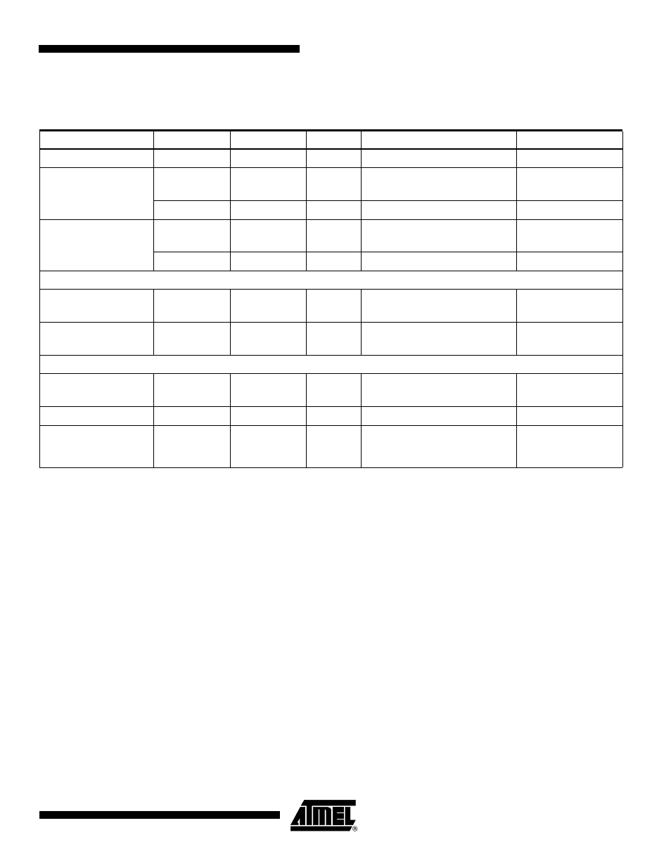
Table 21-5.
CFCE1 and CFCE2 Truth Table
Mode
CFCE2
CFCE1
DBW
Comment
SMC Access Mode
Attribute Memory
NBS1
NBS0
16 bits
Access to Even Byte on D[7:0]
Byte Select
Common Memory
NBS1
NBS0
16 bits
Access to Even Byte on D[7:0]
Access to Odd Byte on D[15:8]
Byte Select
1
0
8 bits
Access to Odd Byte on D[7:0]
I/O Mode
NBS1
NBS0
16 bits
Access to Even Byte on D[7:0]
Access to Odd Byte on D[15:8]
Byte Select
1
0
8 bits
Access to Odd Byte on D[7:0]
True IDE Mode
Task File
1
0
8 bits
Access to Even Byte on D[7:0]
Access to Odd Byte on D[7:0]
Data Register
1
0
16 bits
Access to Even Byte on D[7:0]
Access to Odd Byte on D[15:8]
Byte Select
Alternate True IDE Mode
Control Register
Alternate Status Read
0
1
Don’t
Care
Access to Even Byte on D[7:0]
Don’t Care
Drive Address
0
1
8 bits
Access to Odd Byte on D[7:0]
Standby Mode or
Address Space is not
assigned to CF
1
1
–
–
–