6 plla and pllb characteristics, 7 utmi pll characteristics – Rainbow Electronics AT91CAP9S250A User Manual
Page 964
964
6264A–CAP–21-May-07
AT91CAP9S500A/AT91CAP9S250A
Note:
These characteristics apply only when Main Oscillator is in Bypass Mode (i.e., when MOSCEN = 0 and OSCBYPASS = 1) in the
CKGR_MOR register. See PMC Clock Generator Main Oscillator Register in
Section 29. ”Power Management Controller
.
47.6
PLLA and PLLB Characteristics
The PLLA and PLLB are identical and their characteristics are described in
.
The following characteristics are applicable to the operating temperature range: T
A
= -40°C to 85°C and worst case of
power supply, unless otherwise specified.
Note:
1. Startup time depends on PLL RC filter. A calculation tool is provided by Atmel.
47.7
UTMI PLL Characteristics
The following characteristics are applicable to the operating temperature range: T
A
= -40°C to 85°C and worst case of
power supply, unless otherwise specified.
t
CLXIN
XIN Clock Low Half-period
0.4 x t
CPXIN
0.6 x t
CPXIN
C
IN
XIN Input Capacitance
(1)
5
pF
R
IN
XIN Pulldown Resistor
(1)
500
k
Ω
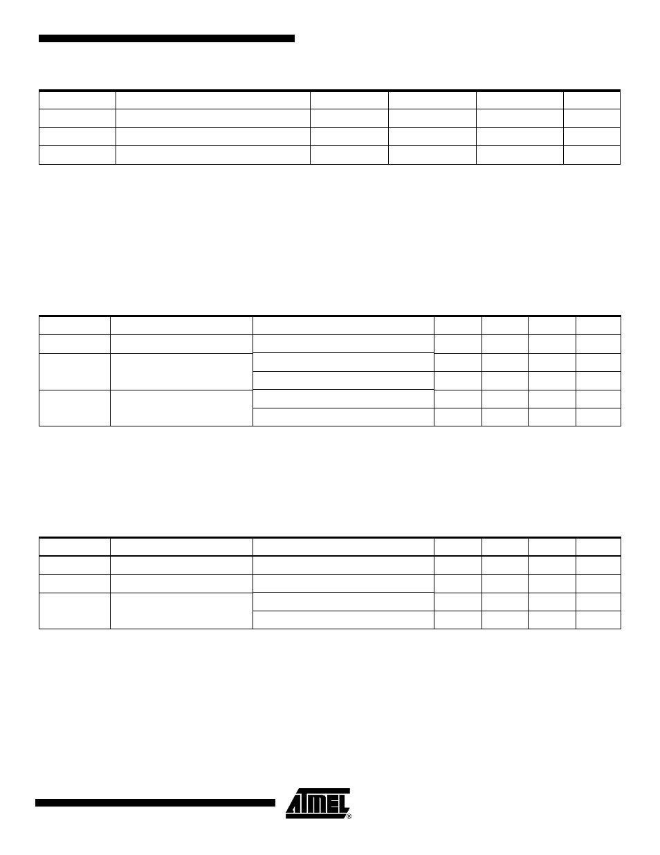
Table 47-9.
Phase Lock Loop A and B Characteristics
Symbol
Parameter
Conditions
Min
Typ
Max
Unit
F
IN
Input Frequency
1
32
MHz
F
OUT
Output Frequency
Field OUT of CKGR_PLL is 00
80
200
MHz
Field OUT of CKGR_PLL is 10
190
240
MHz
I
PLL
Current Consumption
active mode
3
mA
standby mode
1
µA
Table 47-10. Phase Lock Loop Characteristics
Symbol
Parameter
Conditions
Min
Typ
Max
Unit
F
IN
Input Frequency
4
12
32
MHz
F
OUT
Output Frequency
450
480
600
MHz
I
PLL
Current Consumption
active mode
5
8
mA
standby mode
TBD
µA
Table 47-8.
XIN Clock Electrical Characteristics in Bypass Mode
Symbol
Parameter
Conditions
Min
Max
Units