9 adc – Rainbow Electronics AT91CAP9S250A User Manual
Page 967
967
6264A–CAP–21-May-07
AT91CAP9S500A/AT91CAP9S250A
47.9
ADC
Notes:
1. Corresponds to 13 clock cycles at 5 MHz: 3 clock cycles for track and hold acquisition time and 10 clock cycles for
conversion.
The user can drive ADC input with impedance up to:
• Z
OUT
≤
(SHTIM -500) x 12.5
with SHTIM (Sample and Hold Time register) expressed in ns and Z
OUT
expressed in ohms.
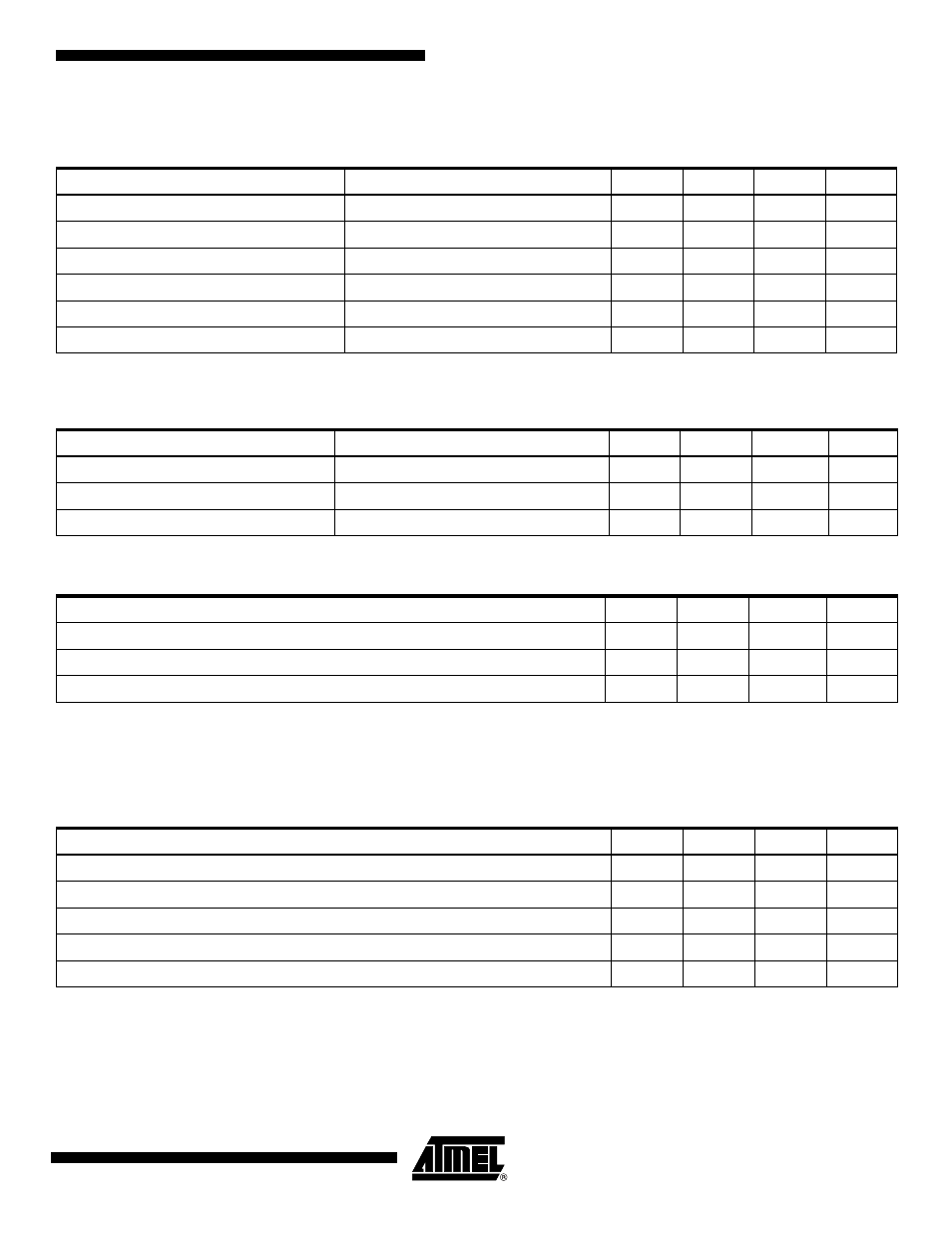
Table 47-14. Channel Conversion Time and ADC CLock
Parameter
Conditions
Min
Typ
Max
Units
ADC Clock Frequency
10-bit resolution mode
5
MHz
ADC Clock Frequency
8-bit resolution mode
TBD
MHz
Startup Time
Return from Idle Mode
40
µs
Track and Hold Acquisition Time
500
ns
Conversion Time
ADC Clock = 5 MHz
2
µs
Throughput Rate
ADC Clock = 5 MHz
384
kSPS
Table 47-15. External Voltage Reference Input
Parameter
Conditions
Min
Typ
Max
Units
ADVREF Input Voltage Range
2.6
VDDANA
V
ADVREF Average Current
On 13 samples with ADC Clock = 5 MHz
250
µA
Current Consumption on VDDANA
300
µA
Table 47-16. Analog Inputs
Parameter
Min
Typ
Max
Units
Input Voltage Range
0
ADVREF
Input Leakage Current
1
µA
Input Capacitance
5
pF
Table 47-17. Transfer Characteristics
Parameter
Min
Typ
Max
Units
Resolution
10
Bit
Integral Non-linearity
±2
LSB
Differential Non-linearity
±0.9
LSB
Offset Error
-1.5
0.5
2.5
LSB
Gain Error
±2
LSB