4 signal description, 5 product dependencies, 1 i/o lines – Rainbow Electronics AT91CAP9S250A User Manual
Page 459: 2 power management, 3 interrupt, 6 functional description, 1 modes of operation, 2 data transfer
459
6264A–CAP–21-May-07
AT91CAP9S500A/AT91CAP9S250A
33.4
Signal Description
33.5
Product Dependencies
33.5.1
I/O Lines
The pins used for interfacing the compliant external devices may be multiplexed with PIO
lines. The programmer must first program the PIO controllers to assign the SPI pins to their
peripheral functions.
33.5.2
Power Management
The SPI may be clocked through the Power Management Controller (PMC), thus the program-
mer must first configure the PMC to enable the SPI clock.
33.5.3
Interrupt
The SPI interface has an interrupt line connected to the Advanced Interrupt Controller (AIC).
Handling the SPI interrupt requires programming the AIC before configuring the SPI.
33.6
Functional Description
33.6.1
Modes of Operation
The SPI operates in Master Mode or in Slave Mode.
Operation in Master Mode is programmed by writing at 1 the MSTR bit in the Mode Register.
The pins NPCS0 to NPCS3 are all configured as outputs, the SPCK pin is driven, the MISO
line is wired on the receiver input and the MOSI line driven as an output by the transmitter.
If the MSTR bit is written at 0, the SPI operates in Slave Mode. The MISO line is driven by the
transmitter output, the MOSI line is wired on the receiver input, the SPCK pin is driven by the
transmitter to synchronize the receiver. The NPCS0 pin becomes an input, and is used as a
Slave Select signal (NSS). The pins NPCS1 to NPCS3 are not driven and can be used for
other purposes.
The data transfers are identically programmable for both modes of operations. The baud rate
generator is activated only in Master Mode.
33.6.2
Data Transfer
Four combinations of polarity and phase are available for data transfers. The clock polarity is
programmed with the CPOL bit in the Chip Select Register. The clock phase is programmed
with the NCPHA bit. These two parameters determine the edges of the clock signal on which
data is driven and sampled. Each of the two parameters has two possible states, resulting in
Table 33-1.
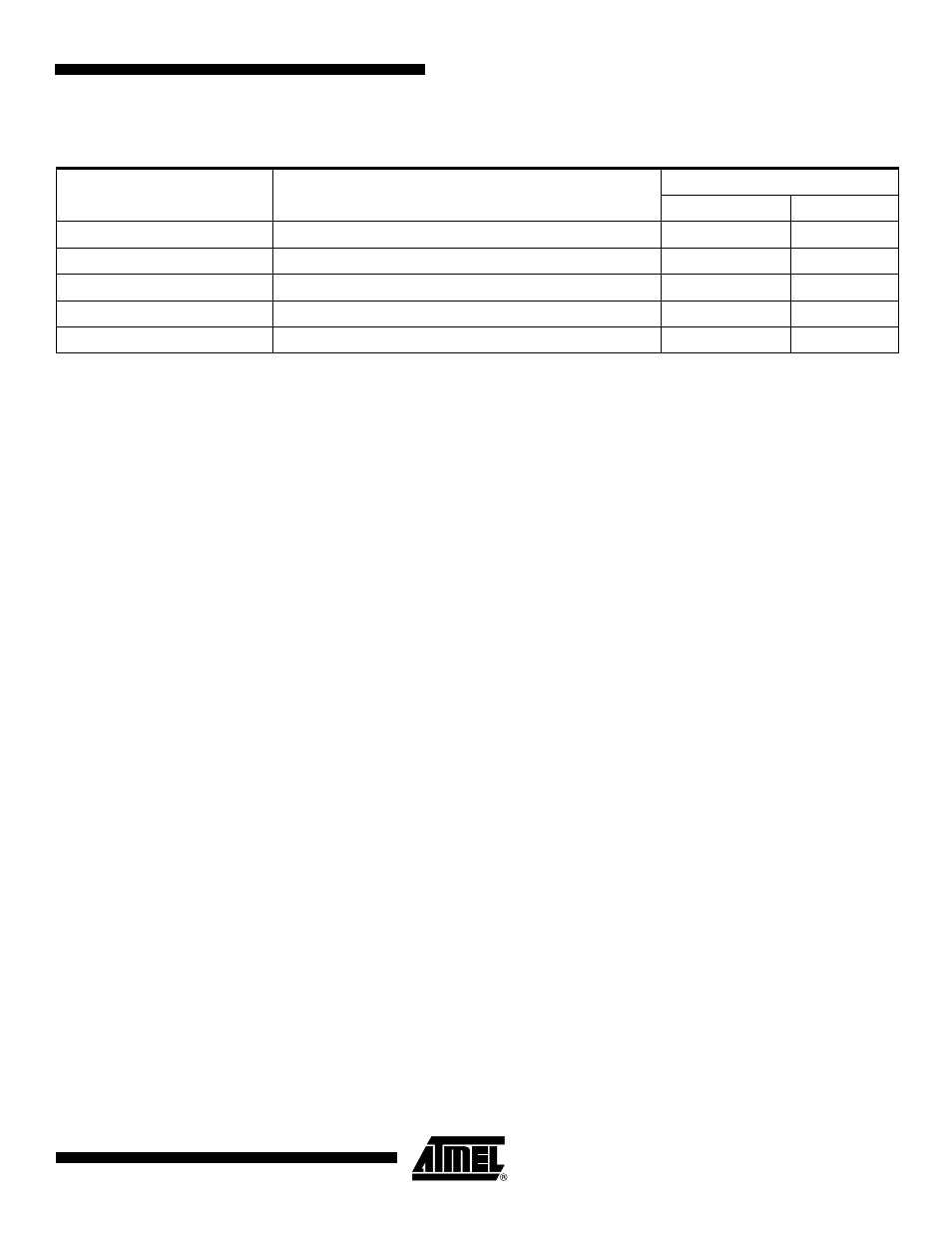
Signal Description
Pin Name
Pin Description
Type
Master
Slave
MISO
Master In Slave Out
Input
Output
MOSI
Master Out Slave In
Output
Input
SPCK
Serial Clock
Output
Input
NPCS1-NPCS3
Peripheral Chip Selects
Output
Unused
NPCS0/NSS
Peripheral Chip Select/Slave Select
Output
Input