5 coding timing parameters, Figure 22-15 – Rainbow Electronics AT91CAP9S250A User Manual
Page 183
183
6264A–CAP–21-May-07
AT91CAP9S500A/AT91CAP9S250A
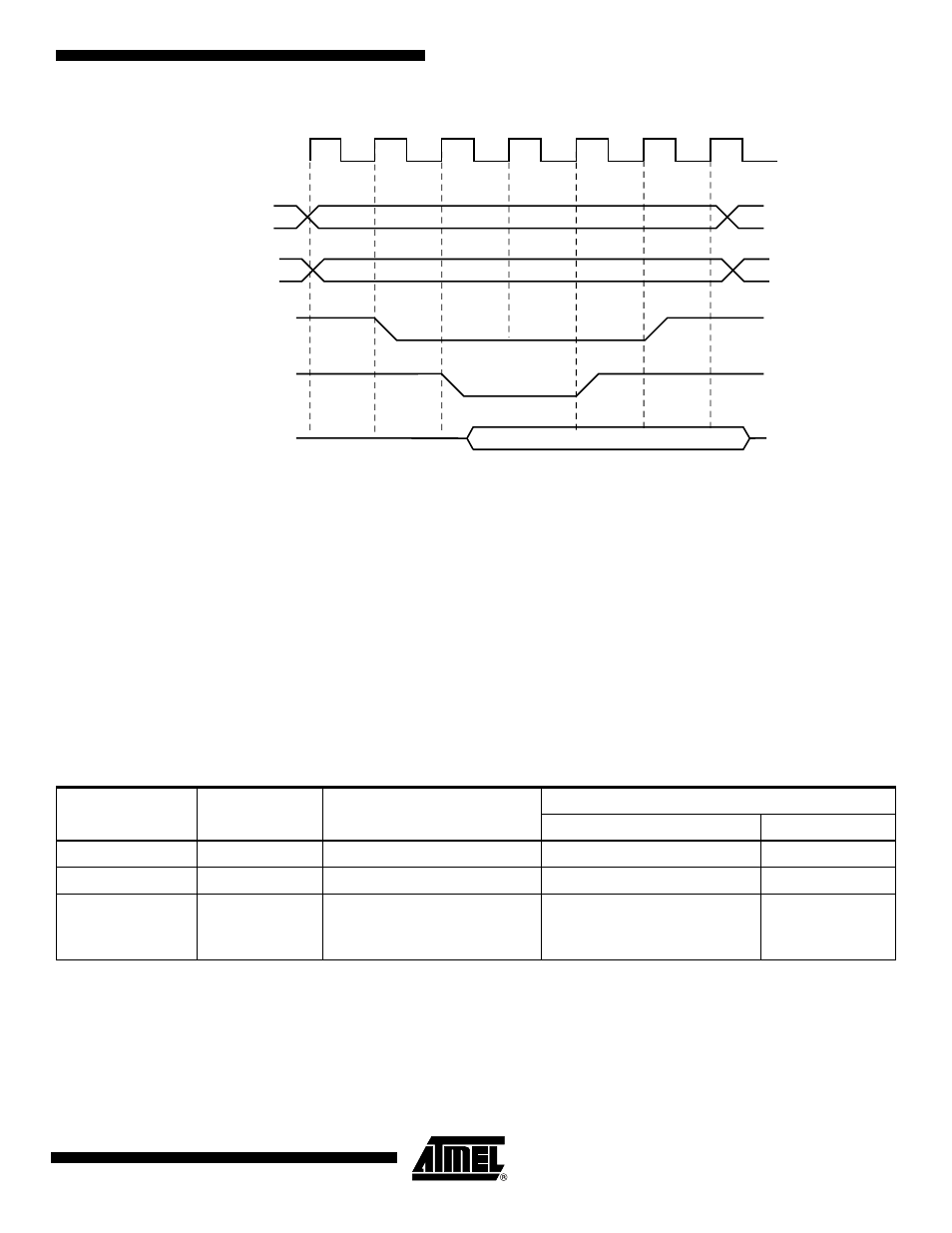
Figure 22-15. WRITE_MODE = 0. The write operation is controlled by NCS
22.8.5
Coding Timing Parameters
All timing parameters are defined for one chip select and are grouped together in one
SMC_REGISTER according to their type.
The SMC_SETUP register groups the definition of all setup parameters:
• NRD_SETUP, NCS_RD_SETUP, NWE_SETUP, NCS_WR_SETUP
The SMC_PULSE register groups the definition of all pulse parameters:
• NRD_PULSE, NCS_RD_PULSE, NWE_PULSE, NCS_WR_PULSE
The SMC_CYCLE register groups the definition of all cycle parameters:
• NRD_CYCLE, NWE_CYCLE
shows how the timing parameters are coded and their permitted range.
MCK
D[31:0]
NCS
NWE,
NWR0, NWR1,
NWR2, NWR3
A
[25:2]
NBS0, NBS1,
NBS2, NBS3,
A0, A1
Table 22-4.
Coding and Range of Timing Parameters
Coded Value
Number of Bits
Effective Value
Permitted Range
Coded Value
Effective Value
setup [5:0]
6
128 x setup[5] + setup[4:0]
0
≤
≤
31
128
≤
≤
128+31
pulse [6:0]
7
256 x pulse[6] + pulse[5:0]
0
≤
≤
63
256
≤
≤
256+63
cycle [8:0]
9
256 x cycle[8:7] + cycle[6:0]
0
≤
≤
127
256
≤
≤
256+127
512
≤
≤
512+127
768
≤
≤
768+127