Rainbow Electronics AT91CAP9S250A User Manual
Page 217
217
6264A–CAP–21-May-07
AT91CAP9S500A/AT91CAP9S250A
For a definition of timing parameters, refer to
Section 23.6.4 ”DDRSDRC Timing 0 Parameter
Write accesses to the SDRAM devices are burst oriented and the burst length is programmed to
8. It determines the maximum number of column locations that can be accessed for a given write
command. When the write command is issued, 8 columns are selected. All accesses for that
burst take place within these eight columns, thus the burst wraps within these 8 columns if a
boundary is reached. These 8 columns are selected by addr[13:3]. addr[2:0] is used to select the
starting location within the block.
In the case of incrementing burst (INCR/INCR4/INCR8/INCR16), the addresses can cross the
16-byte boundary of the SDRAM device. For example, in the case of DDR-SDRAM devices,
when a transfer (INCR4) starts at address 0x0C, the next access is 0x10, but since the burst
length is programmed to 8, the next access is at 0x00. Since the boundary is reached, the burst
is wrapping. The DDRSDRC takes this feature of the SDRAM device into account. In the case of
transfer starting at address 0x04/0x08/0x0C (DDR-SDRAM devices) or starting at address
0x10/0x14/0x18/0x1C, two write commands are issued to avoid to wrap when the boundary is
reached. The last write command is subject to DM input logic level. If DM is registered high, the
corresponding data input is ignored and write access is not done. This avoids additional writing
being done.
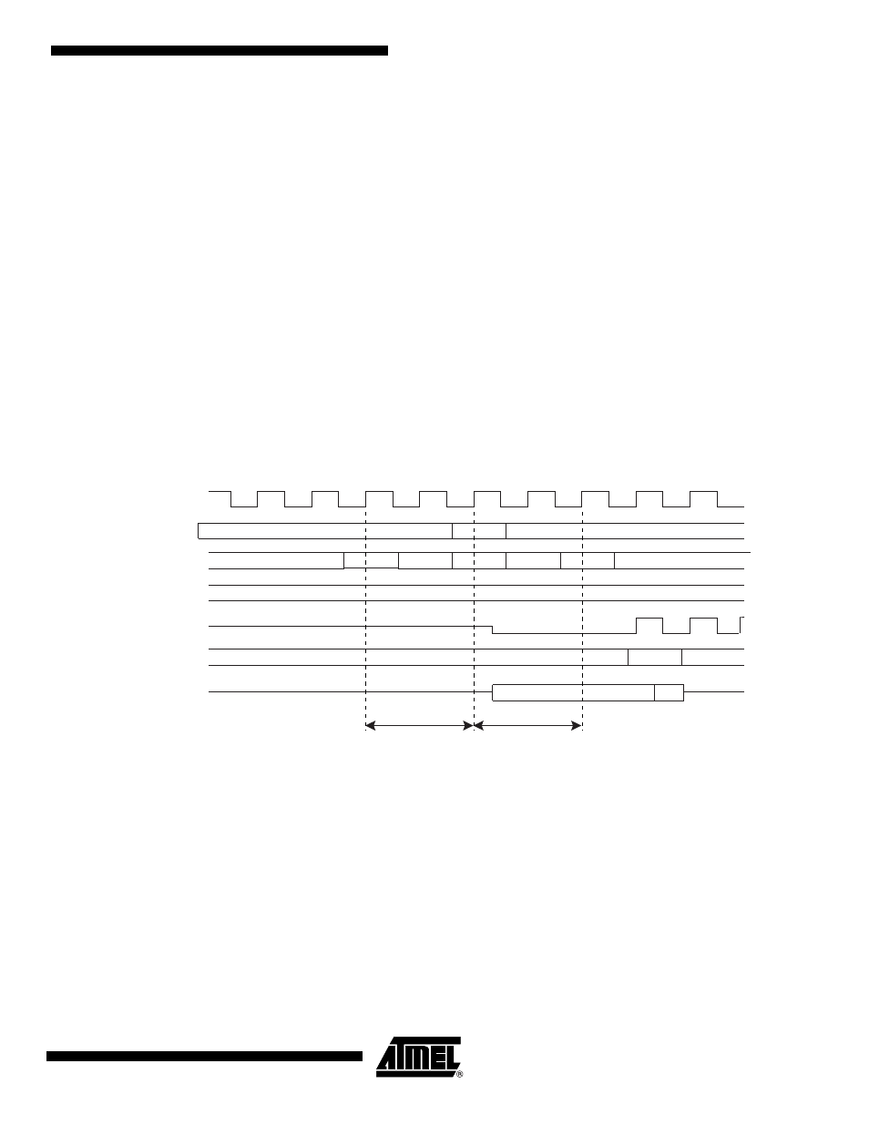
Figure 23-2. Single Write Access, Row Closed, DDR-SDRAM Device
SDCLK
A[12:0]
COMMAND
BA[1:0]
0
Row a
col a
NOP
PRCHG
NOP
ACT
NOP
WRITE
NOP
0
DM[1:0]
0
3
Trp=2
Trcd=2
DQS[1:0]
D[15:0]
Db
Da
3