8 standard read and write protocols – Rainbow Electronics AT91CAP9S250A User Manual
Page 175
175
6264A–CAP–21-May-07
AT91CAP9S500A/AT91CAP9S250A
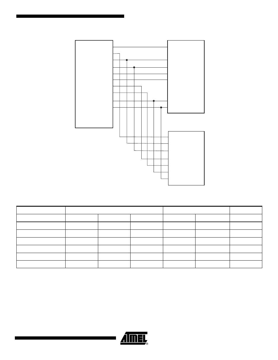
Figure 22-7. Connection of 2x16-bit Data Bus on a 32-bit Data Bus (Byte Select Option)
22.8
Standard Read and Write Protocols
In the following sections, the byte access type is not considered. Byte select lines (NBS0 to
NBS3) always have the same timing as the A address bus. NWE represents either the NWE sig-
nal in byte select access type or one of the byte write lines (NWR0 to NWR3) in byte write
access type. NWR0 to NWR3 have the same timings and protocol as NWE. In the same way,
NCS represents one of the NCS[0..5] chip select lines.
SMC
NWE
NRD
NCS[3]
Write Enable
Read Enable
Memory Enable
NBS0
D[15:0]
D[15:0]
D[31:16]
A[25:2]
A[23:0]
Write Enable
Read Enable
Memory Enable
D[31:16]
A[23:0]
Low Byte Enable
High Byte Enable
Low Byte Enable
High Byte Enable
NBS1
NBS2
NBS3
Table 22-3.
SMC Multiplexed Signal Translation
Signal Name
32-bit Bus
16-bit Bus
8-bit Bus
Device Type
1x32-bit
2x16-bit
4 x 8-bit
1x16-bit
2 x 8-bit
1 x 8-bit
Byte Access Type (BAT)
Byte Select
Byte Select
Byte Write
Byte Select
Byte Write
NBS0_A0
NBS0
NBS0
NBS0
A0
NWE_NWR0
NWE
NWE
NWR0
NWE
NWR0
NWE
NBS1_NWR1
NBS1
NBS1
NWR1
NBS1
NWR1
NBS2_NWR2_A1
NBS2
NBS2
NWR2
A1
A1
A1
NBS3_NWR3
NBS3
NBS3
NWR3