7 multimedia card operations – Rainbow Electronics AT91CAP9S250A User Manual
Page 763
763
6264A–CAP–21-May-07
AT91CAP9S500A/AT91CAP9S250A
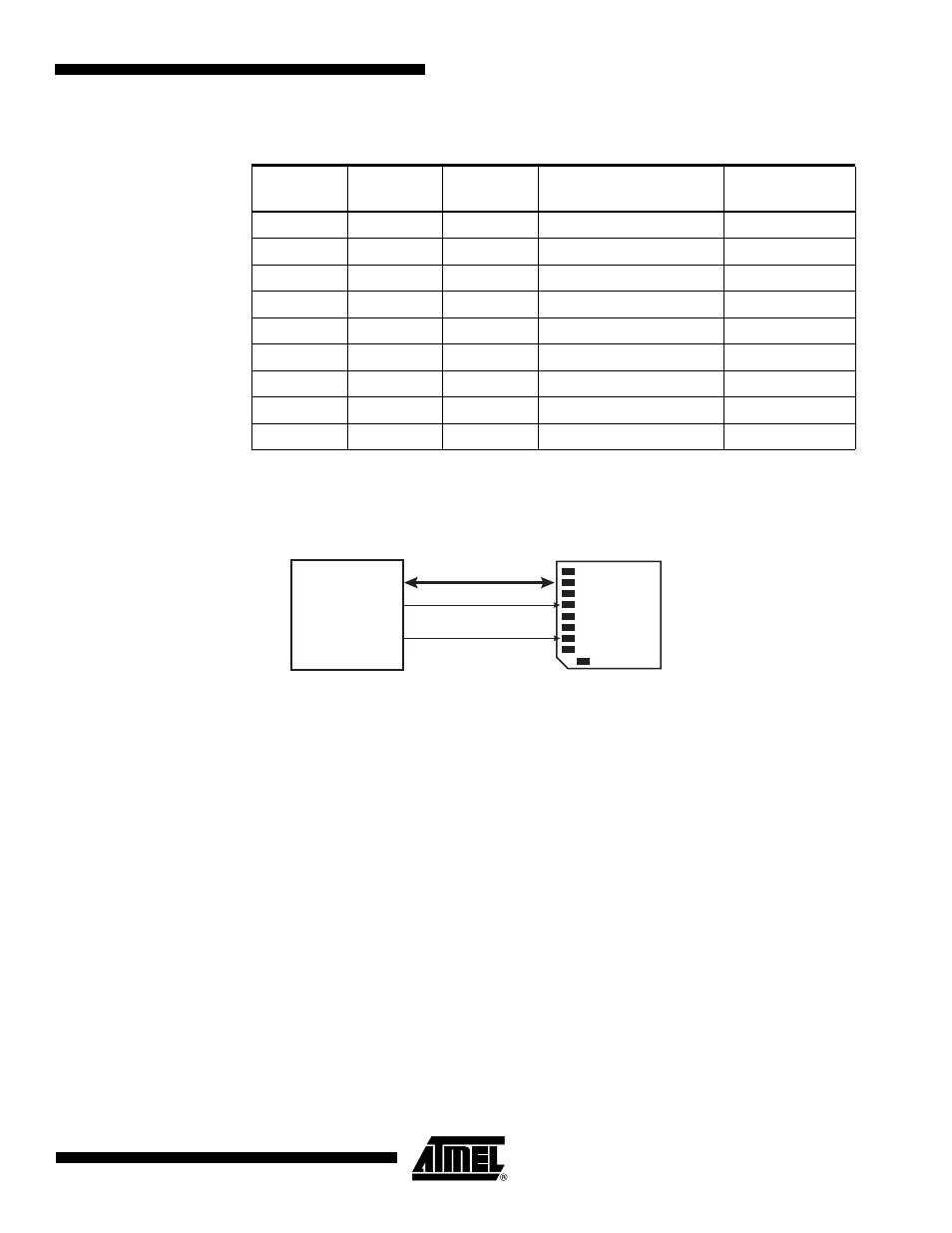
The SD Memory Card bus includes the signals listed in
Notes:
1. I: input, O: output, PP: Push Pull, OD: Open Drain.
2. When several MCI (x MCI) are embedded in a product, MCCK refers to MCIx_CK, MCCDA
to MCIx_CDA, MCDAy to MCIx_DAy.
Figure 41-6. SD Card Bus Connections with One Slot
Note:
When several MCI (x MCI) are embedded in a product, MCCK refers to MCIx_CK, MCCDA to MCIx_CDA MCDAy to MCIx_DAy.
When the MCI is configured to operate with SD memory cards, the width of the data bus can
be selected in the MCI_SDCR register. Clearing the SDCBUS bit in this register means that
the width is one bit; setting it means that the width is four bits. In the case of multimedia cards,
only the data line 0 is used. The other data lines can be used as independent PIOs.
41.7
MultiMedia Card Operations
After a power-on reset, the cards are initialized by a special message-based MultiMedia Card
bus protocol. Each message is represented by one of the following tokens:
• Command: A command is a token that starts an operation. A command is sent from the
host either to a single card (addressed command) or to all connected cards (broadcast
command). A command is transferred serially on the CMD line.
• Response: A response is a token which is sent from an addressed card or (synchronously)
from all connected cards to the host as an answer to a previously received command. A
response is transferred serially on the CMD line.
• Data: Data can be transferred from the card to the host or vice versa. Data is transferred
via the data line.
Table 41-3.
SD Memory Card Bus Signals
Pin
Number
Name
Type
(1)
Description
MCI Pin Name
(2)
(Slot z)
1
CD/DAT[3]
I/O/PP
Card detect/ Data line Bit 3
MCDz3
2
CMD
PP
Command/response
MCCDz
3
VSS1
S
Supply voltage ground
VSS
4
VDD
S
Supply voltage
VDD
5
CLK
I/O
Clock
MCCK
6
VSS2
S
Supply voltage ground
VSS
7
DAT[0]
I/O/PP
Data line Bit 0
MCDz0
8
DAT[1]
I/O/PP
Data line Bit 1 or Interrupt
MCDz1
9
DAT[2]
I/O/PP
Data line Bit 2
MCDz2
2345
6
17
MCDA0 - MCDA3
MCCDA
MCCK
8
SD CARD
9