3 pci cache mode, Table 2.2 pci cache mode alignment, Pci cache mode – Avago Technologies LSI53C1000R User Manual
Page 41: Pci cache mode alignment
PCI Functional Description
2-11
Version 2.2
Copyright © 2000–2003 by LSI Logic Corporation. All rights reserved.
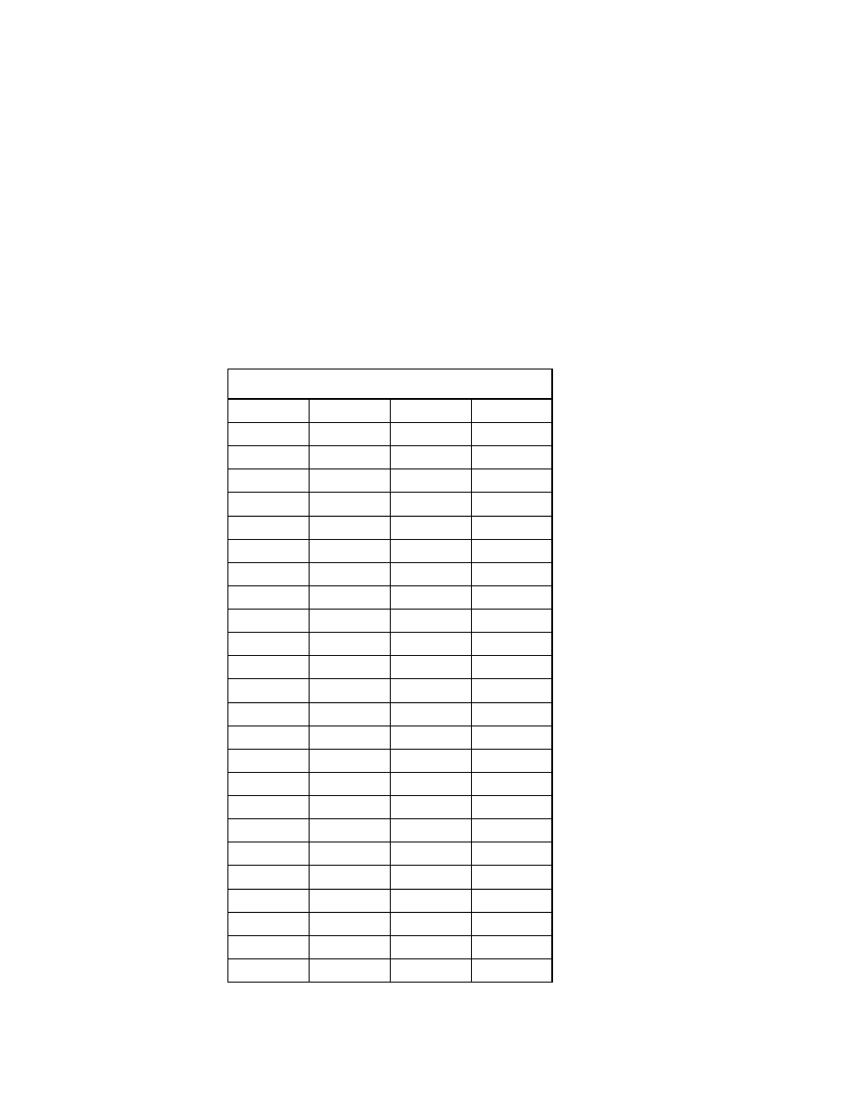
2.1.3 PCI Cache Mode
The LSI53C1000R supports the PCI specification for an 8-bit
register located in the PCI configuration space.
The
register provides the ability to sense and
react to nonaligned addresses corresponding to cache line boundaries.
In conjunction with the
register, the PCI
commands Memory Read Line (MRL), Memory Read Multiple (MRM),
and Memory Write and Invalidate (MWI) are individually software
enabled or disabled.
provides information on the PCI cache
mode alignment.
Table 2.2
PCI Cache Mode Alignment
Host Memory
A
0x00
B
0x04
0x08
C
0x0C
D
0x10
0x14
0x18
0x1C
E
0x20
0x24
0x28
0x2C
F
0x30
0x34
0x38
0x3C
G
0x40
0x44
0x48
0x4C
H
0x50
0x54
0x58
0x5C
0x60
This manual is related to the following products: