Figure6.1 lvd driver, Lvd driver – Avago Technologies LSI53C1000R User Manual
Page 285
DC Characteristics
6-3
Version 2.2
Copyright © 2000–2003 by LSI Logic Corporation. All rights reserved.
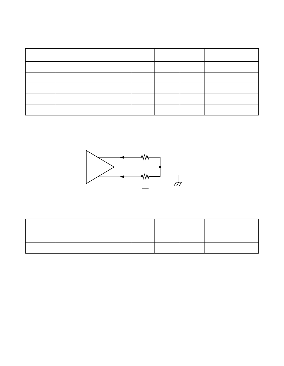
Figure 6.1
LVD Driver
Table 6.3
LVD Driver SCSI Signals
1
– SD[15:0], SDP[1:0], SREQ/, SACK/, SMSG/,
SIO/, SCD/, SATN/, SBSY/, SSEL/, SRST/
1. Note: V
CM
= 0.7–1.8 V (Common Mode, nominal ~1.2 V), R
L
= 0–110
Ω,
R
bias
= 10.0 k
Ω
Symbol
Parameter
Min
Max
Unit
Test Conditions
I
O
+
Source (+) current
−
9.6
−
14.4
mA
Asserted state
I
O
−
Sink (
−
) current
9.6
14.4
mA
Asserted state
I
O
+
Source (+) current
−
6.4
−
9.6
mA
Negated state
I
O
−
Sink (
−
) current
6.4
9.6
mA
Negated state
I
OZ
3-state leakage
–
20
µ
A
–
R
L
2
V
CM
+
I
O
+
R
L
2
I
O
−
−
+
−
Table 6.4
LVD Receiver SCSI Signals
1
– SD[15:0], SDP[1:0], SREQ/, SACK/, SMSG/,
SIO/, SCD/, SATN/, SBSY/, SSEL/, SRST/
1. Note: V
CM
= 0.7–1.8 V (Common Mode Voltage, nominal ~1.2 V.)
Symbol
Parameter
Min
Max
Unit
Test Conditions
V
I
LVD receiver voltage asserting
60
–
mV
Differential voltage
V
I
LVD receiver voltage negating
−
60
–
mV
Differential voltage