Chip control three (ccntl3), Chip control two (ccntl2), Register: 0x5a – Avago Technologies LSI53C1000R User Manual
Page 207: Register: 0x5b
SCSI Registers
4-95
Version 2.2
Copyright © 2000–2003 by LSI Logic Corporation. All rights reserved.
receiving data using programmed I/O. This register can
also be used for diagnostic testing or in the low level mode.
The power-up value of this register is indeterminate.
If the chip is in wide mode (
,
bit 3 is set) and
register is
read, both byte lanes are checked for parity regardless of
phase. When in a nondata phase, this causes a parity
error interrupt to be generated because the upper byte
lane parity is invalid.
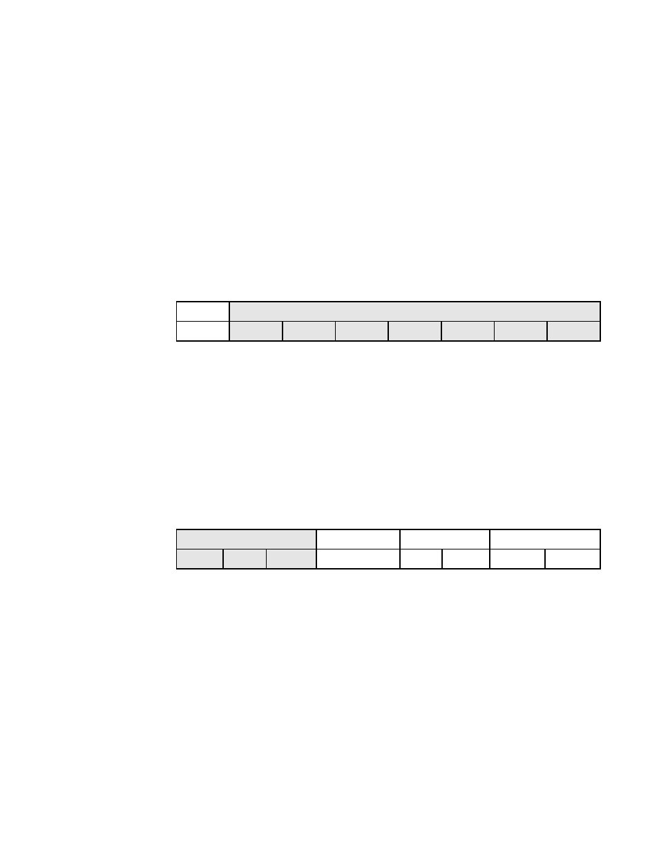
Register: 0x5A
Chip Control Two (CCNTL2)
Read/Write
ShSGE
Enable Shadowed SGE Register
7
Setting this bit allows access to the SGE Status registers
shadowed behind SIST0 and SIST1.
R
Reserved
[6:0]
Register: 0x5B
Chip Control Three (CCNTL3)
Read/Write
R
Reserved
[7:5]
ENDSKEW
Enable REQ/ACK to Data Skew Control
4
Setting this bit enables the control of the relative skew
between the SCSI REQ/ACK signals and the data
signals. The actual amount of skew time is controlled by
DSKEW[1:0] in this register.
7
6
0
ShSGE
R
0
x
x
x
x
x
x
x
7
5
4
3
2
1
0
R
ENDSKEW
DSKEW[1:0]
LVDDL[1:0]
0
0
0
0
0
0
0
0