3 scsi shadow registers, Scsi shadow registers, Section 4.3, “scsi shadow registers – Avago Technologies LSI53C1000R User Manual
Page 237
SCSI Shadow Registers
4-125
Version 2.2
Copyright © 2000–2003 by LSI Logic Corporation. All rights reserved.
4.3 SCSI Shadow Registers
Note:
For more information concerning shadow registers, refer to
the
,
,
,
Memory Move Read Selector (MMRS)
Memory Move Write Selector (MMWS)
and
register descriptions.
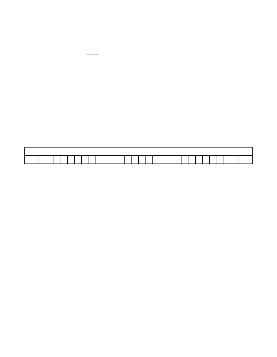
Registers: 0x34–0x37
Shadowed Scratch Register A (SCRATCHA)
Read/Write
SCRATCHA
Scratch Register A
[31:0]
When the Configuration Info Enable bit in the
register is set,
SCRATCH Register A is placed in the shadowed mode
and returns bits [31:10] of the PCI
Base Address Register One (BAR1) (MEMORY)
in bits
[31:10]. Bits [9:0] of SCRATCH A always return zero in
this mode. Writes to the SCRATCHA register have no
effect. Clearing the PCI Configuration Info Enable bit
causes the SCRATCH A register to return to normal
operation.
31
0
SCRATCHA
0
0
0
0
0
0
0
0
0
0
0
0
0
0
0
0
0
0
0
0
0
0
0
0
0
0
0
0
0
0
0
0