Table 4.2 lsi53c875n power and ground signals, Lsi53c875n power and ground signals, Table 4.1 – Avago Technologies LSI8751D User Manual
Page 99
4-7
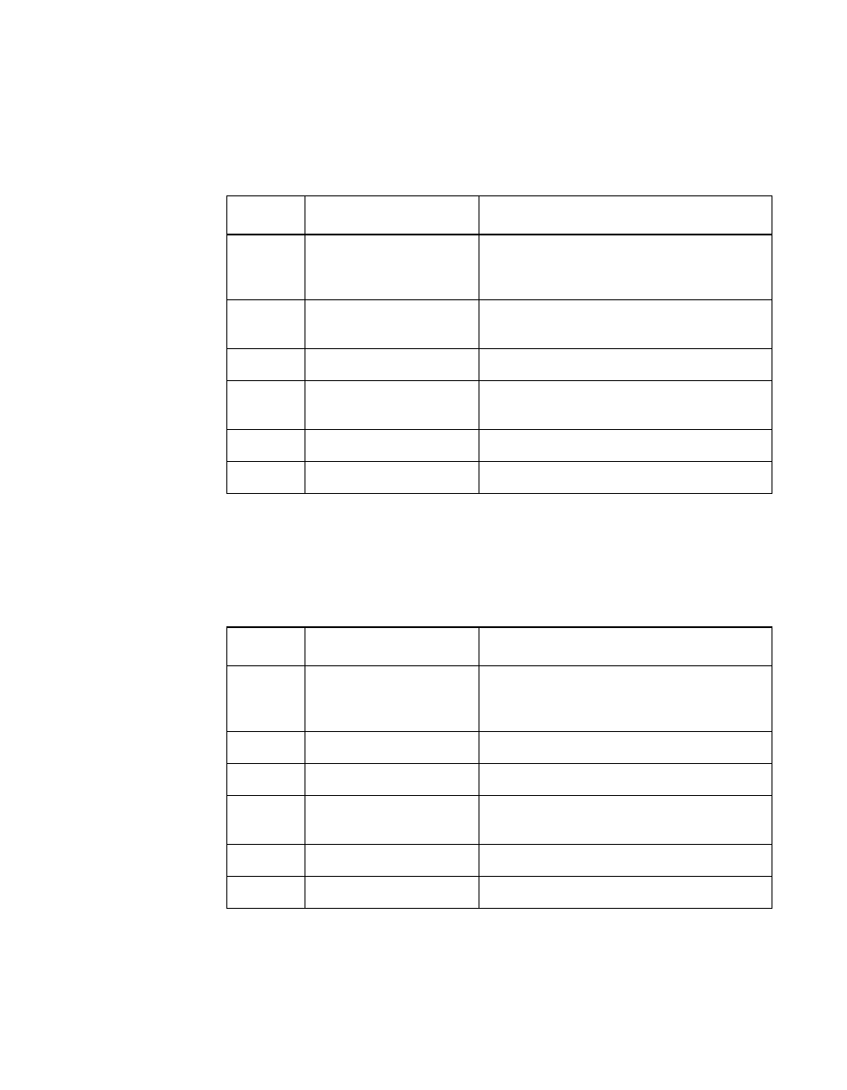
describes the LSI53C875, LSI53C875J, LSI53C875E, and
LSI53C875JE Power and Ground Signals group.
describes the LSI53C875N Power and Ground Signals group.
Table 4.1
LSI53C875, LSI53C875J, LSI53C875E, and LSI53C875JE
Power and Ground Signals
Name
Pin No.
Description
V
SS
4, 10, 14, 18, 23, 27,
31, 37, 42, 48, 69, 79,
123, 133, 152, 158
Ground to the PCI I/O pins.
V
DD
63, 74, 84, 118, 128,
138
Power supplies to the Standard I/O pins.
V
DD-I
1
1. These pins can accept a V
DD
source of 3.3 V or 5 V. All other V
DD
pins must
be supplied 5 V.
8, 21, 33, 45, 155
V
DD
pad for PCI I/O pins.
V
SS
-S
88, 93, 99, 104, 109,
114
Ground to the SCSI bus I/O pins.
V
SS
-C
55, 146
Ground to the internal logic core.
V
DD
-C
51, 149
Power supplies to the internal logic core.
Table 4.2
LSI53C875N Power and Ground Signals
Name
Pin No.
Description
V
SS
10, 16, 20, 24, 29, 33,
38, 44, 59, 65, 88, 98,
164, 175, 196, 202
Ground to the PCI I/O pins.
V
DD
82, 93, 148, 169, 180
Power supplies to the Standard I/O pins.
V
DD-I
1
1. These pins can accept a V
DD
source of 3.3 V or 5 V. All other V
DD
pins must
be supplied 5 V.
14, 27, 62, 199
V
DD
pad for PCI I/O pins.
V
SS
-S
118, 123, 129, 134,
139, 144
Ground to the SCSI bus I/O pins.
V
SS
-C
72, 189
Ground to the internal logic core.
V
DD
-C
68, 192
Power supplies to the internal logic core.