Scsi output data latch (sodl), Scsi output, Data latch (sodl) – Avago Technologies LSI8751D User Manual
Page 194: Scsi output data latch, Sodl), Scsi bus data lines (sbdl), Scsi, Output data latch (sodl), Scsi out, Put data latch (sodl)
5-78
SCSI Operating Registers
Registers: 0x54–0x55 (0xD4–0xD5)
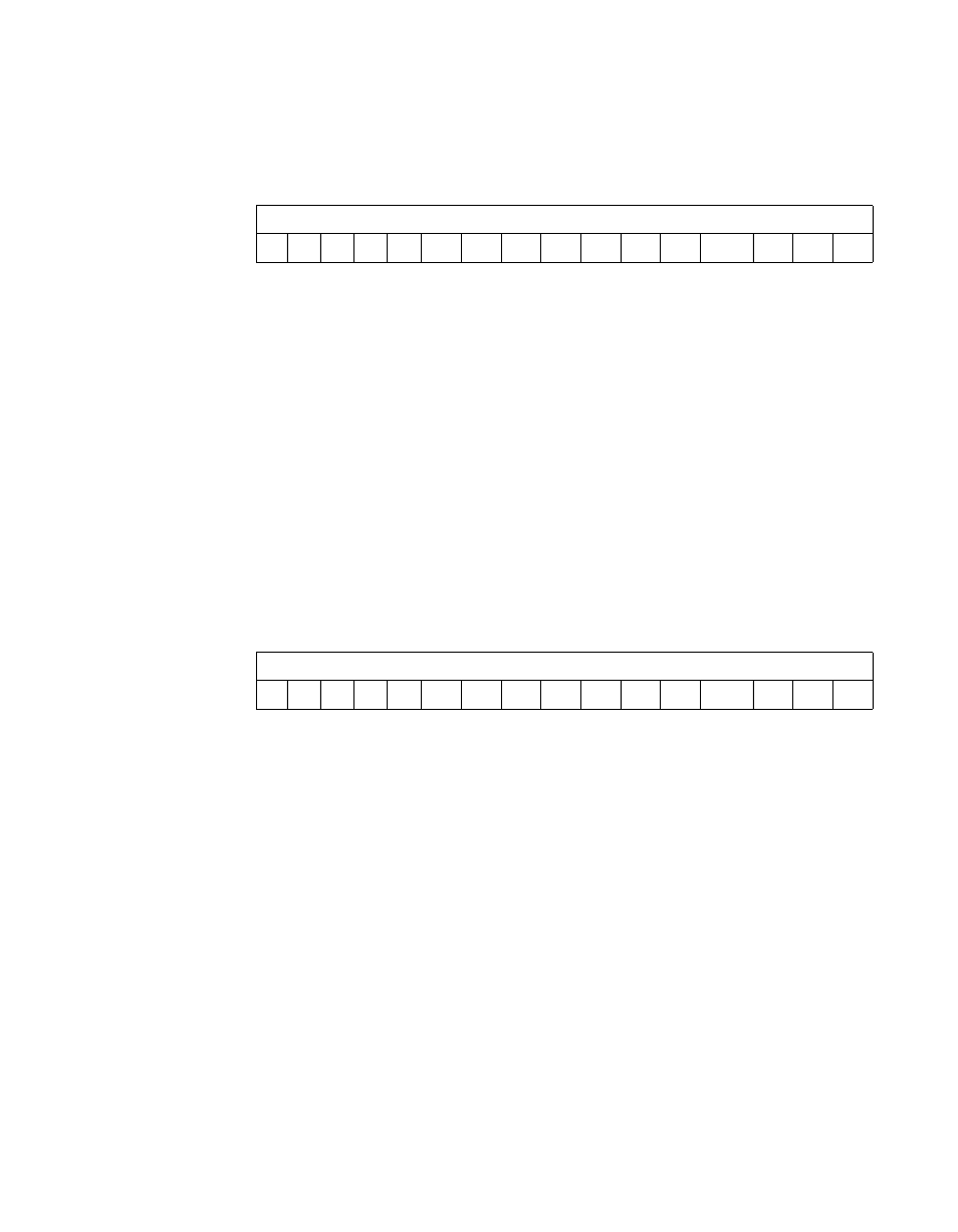
SCSI Output Data Latch (SODL)
Read/Write
SODL
SCSI Output Data Latch
[15:0]
This register is used primarily for diagnostic testing or
programmed I/O operation. Data written to this register is
asserted onto the SCSI data bus by setting the Assert
Data Bus bit in the
register.
This register is used to send data using programmed I/O.
Data flows through this register when sending data in any
mode. It is also used to write to the synchronous data
FIFO when testing the chip. The power-up value of this
register is indeterminate.
Registers: 0x58–0x59 (0xD8–0xD9)
SCSI Bus Data Lines (SBDL)
Read Only
SBDL
SCSI Bus Data Lines
[15:0]
This register contains the SCSI data bus status. Even
though the SCSI data bus is active low, these bits are
active high. The signal status is not latched and is a true
representation of exactly what is on the data bus at the
time the register is read. This register is used when
receiving data using programmed I/O. This register can
also be used for diagnostic testing or in low level mode.
If the chip is in wide mode
, bit 3,
, bit 2 and
is read, both byte lanes are
checked for parity regardless of phase. When in a
nondata phase, this will cause a parity error interrupt to
be generated because upper byte lane parity is invalid.
15
0
SODL
x
x
x
x
x
x
x
x
x
x
x
x
x
x
x
x
15
0
SBDL
x
x
x
x
x
x
x
x
x
x
x
x
x
x
x
x