Figure1.2 lsi53c875 chip block diagram, Lsi53c875 chip block diagram – Avago Technologies LSI8751D User Manual
Page 17
1-3
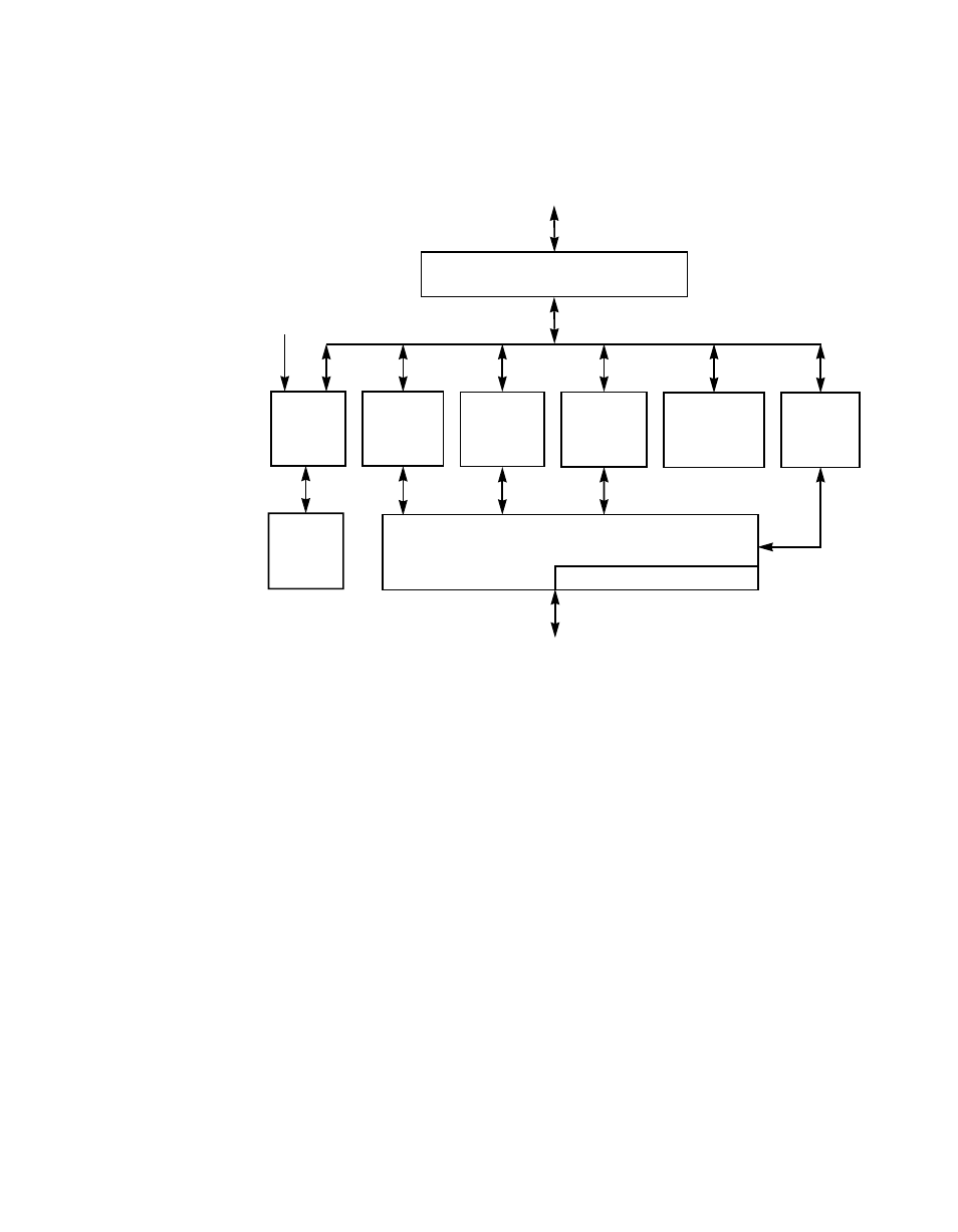
A block diagram of the LSI53C875 is pictured in
Figure 1.2
LSI53C875 Chip Block Diagram
The LSI53C875 integrates a high-performance SCSI core, a PCI bus
master DMA core, and the LSI Logic SCSI SCRIPTS processor to meet
the flexibility requirements of SCSI-3 and Ultra SCSI standards. It is
designed to implement multithreaded I/O algorithms with a minimum of
processor intervention, solving the protocol overhead problems of
previous intelligent and nonintelligent adapter designs.
The LSI53C875 is fully supported by the LSI Logic Storage Device
Management System (SDMS™), a software package that supports the
Advanced SCSI Protocol Interface (ASPI) and the ANSI Common
Access Method (CAM). SDMS software provides BIOS and driver
support for hard disk, tape, removable media products, and CD-ROM
under the major PC operating systems.
PCI Master and Slave Control Block
Data
FIFO
536 Bytes
Memory
Control
SCSI
SCRIPTS
Processor
Operating
Registers
Configuration
Registers
SCRIPTS
RAM
SCSI FIFO and SCSI Control Block
Local
Bus
Memory
TolerANT Drivers and Receivers
SCSI Bus
External
Memory
PCI