Chip test four (ctest4), Chip test four, Ctest4) – Avago Technologies LSI8751D User Manual
Page 156
5-40
SCSI Operating Registers
3.
If the DMA FIFO size is set to 88 bytes, and the
result with 0x7F for a byte count between 0 and 64.
If the DMA FIFO size is set to 536 bytes, and the
result with 0x3FF for a byte count between 0 and
536.
Note:
To calculate the total number of bytes in both the DMA
FIFO and SCSI logic, see the section on Data Paths in
Chapter 2, “Functional Description.”
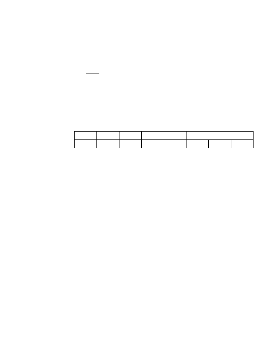
Register: 0x21 (0xA1)
Chip Test Four (CTEST4)
Read/Write
BDIS
Burst Disable
7
When set, this bit causes the LSI53C875 to perform
back-to-back cycles for all transfers. When this bit is
cleared, LSI53C875 back-to-back transfers for opcode
fetches and burst transfers for data moves are per-
formed.
ZMOD
High Impedance Mode
6
Setting this bit causes the LSI53C875 to place all output
and bidirectional pins into a high impedance state. In
order to read data out of the LSI53C875, clear this bit.
This bit is intended for board-level testing only. Do not set
this bit during normal system operation.
ZSD
SCSI Data High Impedance
5
Setting this bit causes the LSI53C875 to place the SCSI
data bus SD[15:0] and the parity lines SDP[1:0] in a high
impedance state. In order to transfer data on the SCSI
bus, clear this bit.
SRTM
Shadow Register Test Mode
4
Setting this bit allows access to the shadow registers
used by Memory-to-Memory Move operations. When this
bit is set, register accesses to the
and
registers are directed to
7
6
5
4
3
2
0
BDIS
ZMOD
ZSD
SRTM
MPEE
FBL[2:0]
0
0
0
0
0
0
0
0