Avago Technologies LSI8751D User Manual
Page 259
PCI and External Memory Interface Timing Diagrams
7-23
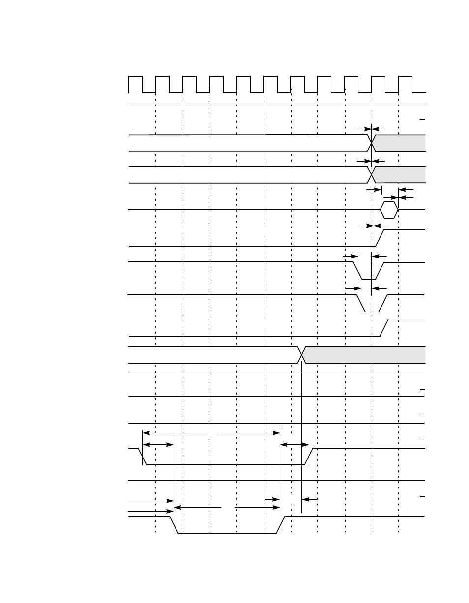
Figure 7.14 External Memory Write (Cont.)
11
12
13
14
15
16
17
18
19
20
t
2
t
2
21
t
1
t
3
t
3
Data In
Byte Enable
In
Data Out
t
20
t
23
CLK
(Driven by System)
PAR
(Driven by Master-Addr;
IRDY/
(Driven by Master)
TRDY/
(Driven by LSI53C875)
STOP/
(Driven by LSI53C875)
DEVSEL/
(Driven by LSI53C875)
AD
(Driven by Master-Addr;
C_BE/
(Driven by Master)
FRAME/
(Driven by Master)
LSI53C875-Data)
LSI53C875-Data)
MAD
(Driven by LSI53C875)
GPIO2_MAS2/
(Driven by LSI53C875)
MAS1/
(Driven by LSI53C875)
MCE/
(Driven by LSI53C875)
MOE/
(Driven by LSI53C875)
MWE/
(Driven by LSI53C875)
MAS0/
(Driven by LSI53C875)
t
2
t
2
t
22
t
21
t
26
t
24
t
25
This manual is related to the following products:
See also other documents in the category Avago Technologies Hardware:
- MGA-725M4 (4 pages)
- MGA-71543 (4 pages)
- MGA-71543 (3 pages)
- MGA-82563 (6 pages)
- 3ware SAS 9750-8i (48 pages)
- 3ware 9690SA-8I (Channel) (138 pages)
- 3ware 9690SA-8I (Channel) (380 pages)
- 3ware SAS 9750-8i (29 pages)
- 3ware 9550SXU-8LP (Channel) (149 pages)
- 3ware 9550SXU-8LP (Channel) (40 pages)
- 3ware 9650SE-8LPML (Channel) (45 pages)
- 3ware 9690SA-8I (Channel) (27 pages)
- 3ware 9690SA-8I (Channel) (361 pages)
- 6160 SAS Switch (2 pages)
- Cache Protection for RAID Controller Cards (139 pages)
- Cache Protection for RAID Controller Cards (13 pages)
- MegaRAID SAS 9271-8iCC (13 pages)
- MegaRAID SAS 9361-8i (13 pages)
- MegaRAID SAS 9266-8i (12 pages)
- MegaRAID SAS 9380-8e (43 pages)
- MegaRAID SAS 9271-8iCC (26 pages)
- MegaRAID SafeStore Software (502 pages)
- MegaRAID SAS 9285-8ecv (80 pages)
- MegaRAID SAS 9285-8ecv (92 pages)
- MegaRAID SAS 9266-8i (20 pages)
- MegaRAID SAS 0260CV-4i (49 pages)
- MegaRAID SAS 9271-8i (8 pages)
- MegaRAID SAS 0260CV-4i (72 pages)
- MegaRAID SAS 0260CV-4i (64 pages)
- MegaRAID SAS 9361-8i (7 pages)
- MegaRAID SAS 9341-8i (8 pages)
- MegaRAID SAS 9380-4i4e (7 pages)
- MegaRAID SAS 9380-8e (7 pages)
- MegaRAID SAS 0260CV-4i (28 pages)
- MegaRAID SAS 9240-8i (4 pages)
- MegaRAID SAS 9280-24i4e (14 pages)
- MegaRAID SAS 9280-24i4e (16 pages)
- MegaRAID SAS 9260-16i (12 pages)
- MegaRAID SAS 9280-8e (22 pages)
- MegaRAID SAS 9260-8i (4 pages)
- MegaRAID SafeStore Software (8 pages)
- MegaRAID SAS 9261-8i (4 pages)
- MegaRAID SAS 9285-8e (12 pages)
- MegaRAID SAS 9280-16i4e (12 pages)
- MegaRAID SAS 9280-4i4e (4 pages)