1 mad bus programming, Mad bus programming, Section 4.1, “mad bus program – Avago Technologies LSI8751D User Manual
Page 114: Ming, Table 4.12
4-22
Signal Descriptions
describes the JTAG Signals group for the LSI53C875J,
LSI53C875N, and LSI53C875JB.
4.1 MAD Bus Programming
The MAD[7:0] pins, in addition to serving as the address/data bus for the
local memory interface, are also used to program power-up options for
the chip. A particular option is programmed by connecting a 4.7 k
Ω
resistor between the appropriate MAD[x] pin and Vss. The pull-down
resistors require that HC or HCT external components are used for the
memory interface.
•
MAD[7] has no functionality. Do not place a pull-down resistor on
this pin.
GPIO2_
MAS2/
68 /87/J8
I/O
General Purpose I/O pin. Optionally, this pin is used as a
Memory Address Strobe 2 if an external memory with more than
16 bits of addressing is specified by the pull-down resistors at
power-up and bit 0 in the
register
is set.
Table 4.11
External Memory Interface Signals (Cont.)
Name
Pin No.
LSI53C875,
LSI53C875J,
LSI53C875N,
LSI53C875JB
Typ
e
Description
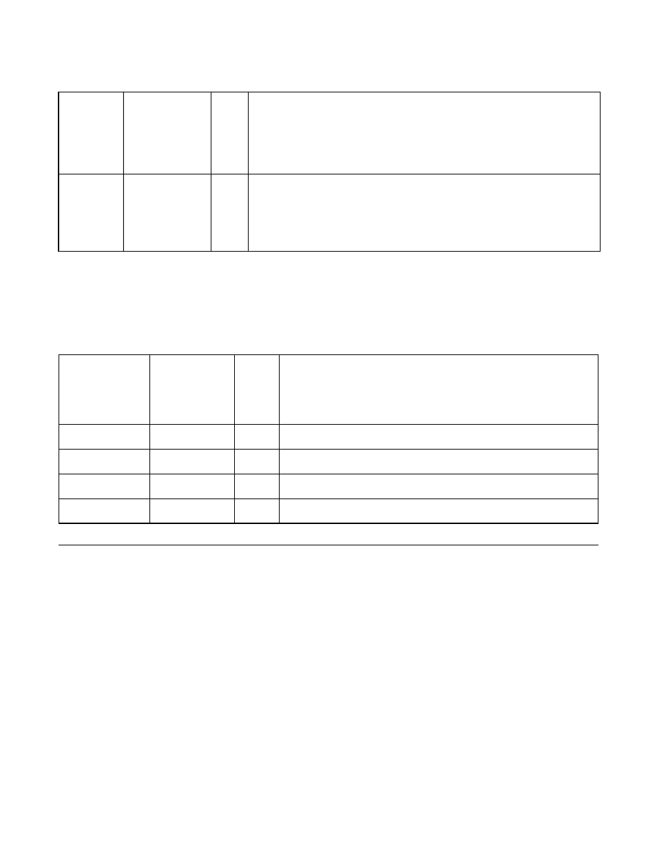
Table 4.12
JTAG Signals (LSI53C875J/LSI53C875N/LSI53C875JB Only)
Name
Pin No.
LSI53C875J,
LSI53C875N,
LSI53C875JB
Type
Description
TCK
130/172/A10
–
Test Clock pin for JTAG boundary scan.
TMS
57/75/N6
–
Test Mode Select pin for JTAG boundary scan.
TDI
142/185/D7
–
Test Data In pin for JTAG boundary scan.
TDO
58/77/J6
–
Test Data Out pin for JTAG boundary scan.