Dma control, Dcntl), Dma control (dcntl) – Avago Technologies LSI8751D User Manual
Page 167: Control (dcntl), Register: 0x3a (0xba), Register: 0x3b (0xbb)
5-51
For more information on interrupts, see
Register: 0x3A (0xBA)
Scratch Byte Register (SBR)
Read/Write
This is a general purpose register. Apart from CPU access, only register
Read/Write and Memory Moves into this register will alter its contents.
The default value of this register is zero. This register was called the
DMA Watchdog Timer on previous LSI53C8XX family products.
Register: 0x3B (0xBB)
DMA Control (DCNTL)
Read/Write
CLSE
Cache Line Size Enable
7
Setting this bit enables the LSI53C875 to sense and
react to cache line boundaries set up by the DMODE or
PCI
register, whichever contains the
smaller value. Clearing this bit disables the cache line
size logic and the LSI53C875 monitors the cache line
size using the
register.
PFF
Prefetch Flush
6
Setting this bit causes the prefetch unit to flush its
contents. The bit clears after the flush is complete.
PFEN
Prefetch Enable
5
Setting this bit enables the prefetch unit if the burst size
is equal to or greater than four. For more information on
SCRIPTS instruction prefetching, see
SSM
Single Step Mode
4
Setting this bit causes the LSI53C875 to stop after
executing each SCRIPTS instruction, and generates a
single step interrupt. When this bit is cleared, the
LSI53C875 does not stop after each instruction. It
7
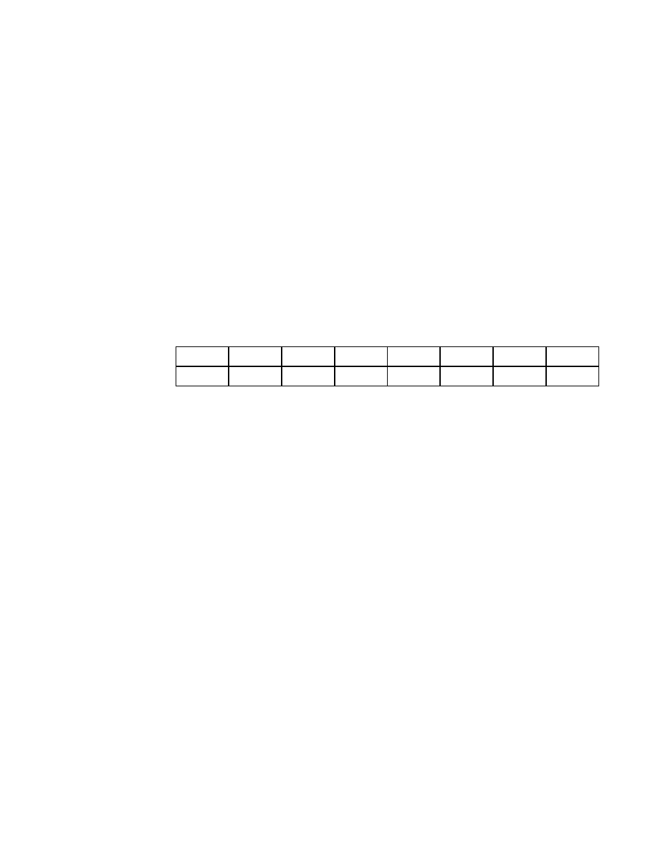
6
5
4
3
2
1
0
CLSE
PFF
PFEN
SSM
IRQM
STD
IRQD
COM
0
0
0
0
0
0
0
0