Figure7.1 rise and fall time test conditions, Figure7.2 scsi input filtering, Rise and fall time test conditions – Avago Technologies LSI8751D User Manual
Page 244: Scsi input filtering, Figure 7.1
7-8
Instruction Set of the I/O Processor
Figure 7.1
Rise and Fall Time Test Conditions
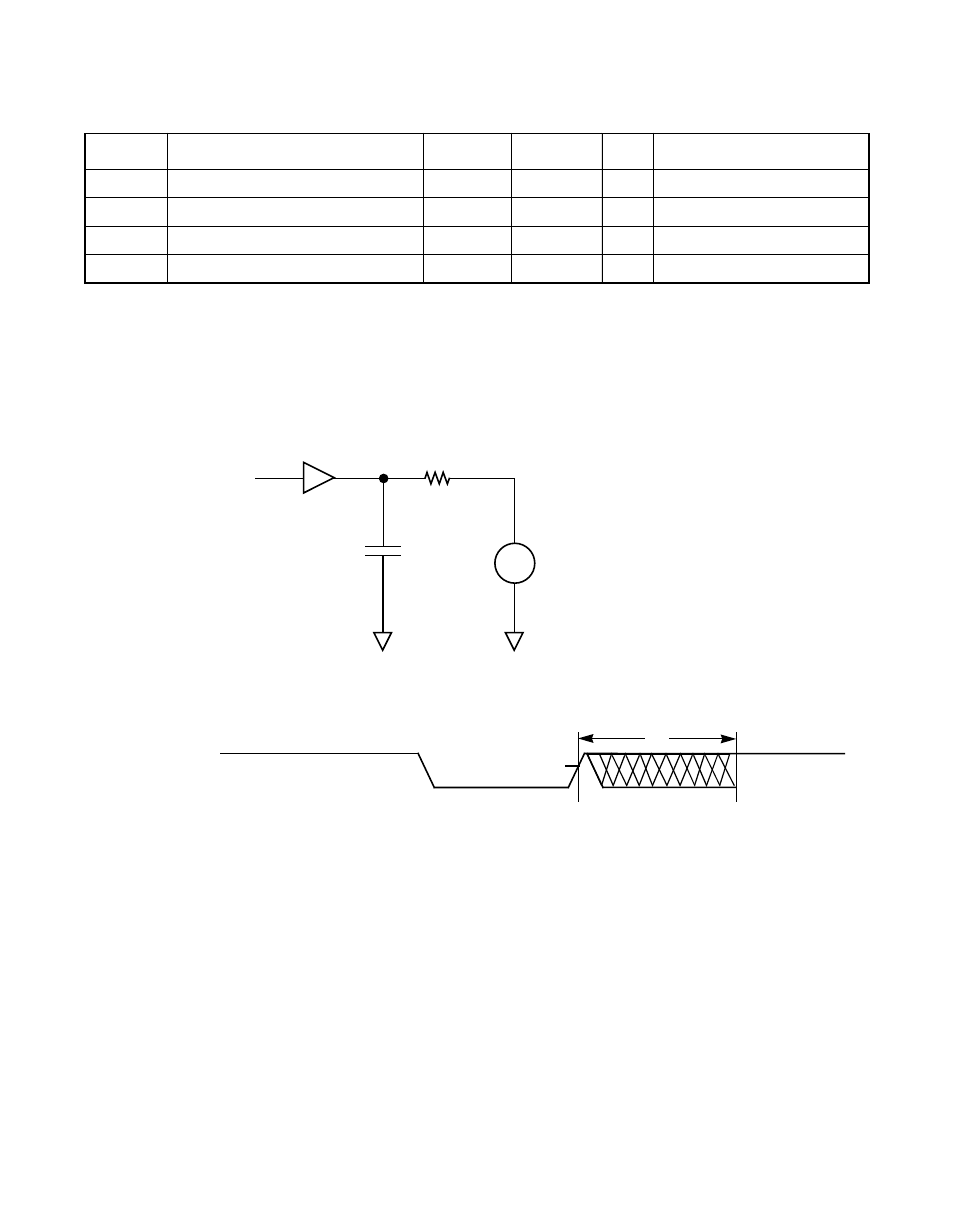
Figure 7.2
SCSI Input Filtering
ESD
Electrostatic discharge
2
–
kV
MIL-STD-883C; 3015-7
Latch-up
100
–
mA
–
Filter delay
20
30
ns
Extended filter delay
40
60
ns
1. Active negation outputs only: Data, Parity, SREQ/, SACK/.
2. Single pin only; irreversible damage may occur if sustained for one second.
3. SCSI RESET pin has 10 k
Ω
pull-up resistor.
Note: These values are guaranteed by periodic characterization; they are not 100% tested on every
device.
Table 7.15
TolerANT Technology Electrical Characteristics
Symbol
Parameter
Min
Max
Unit
Test Conditions
2.5 V
47
Ω
20 pF
+
−
REQ/ or ACK/ Input
t
1
V
TH
Note: t
1
is the input filtering period.
This manual is related to the following products: