Table 7.18 interrupt output, Figure7.8 interrupt output, Pci and external memory interface timing diagrams – Avago Technologies LSI8751D User Manual
Page 249: Interrupt output
PCI and External Memory Interface Timing Diagrams
7-13
and
provide Interrupt Output timing data.
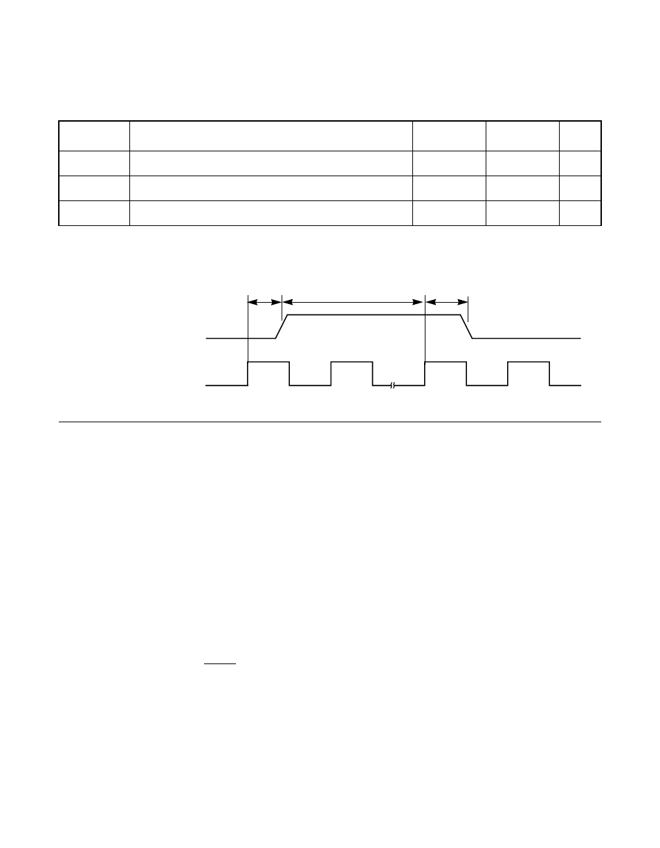
Figure 7.8
Interrupt Output
7.4 PCI and External Memory Interface Timing Diagrams
through
represent signal activity when the
LSI53C875 accesses the PCI bus. The timings for the PCI and external
memory buses are listed on
. This section includes timing
diagrams for access to three groups of external memory configurations.
The first group applies to systems with memory size of 64 Kbytes and
above; one byte read or write cycle, and fast or normal ROMs. The
second group applies to systems with memory size of 64 Kbytes and
above, one byte read or write cycles, and slow ROMs. The third group
applies to systems with memory size of 64 Kbytes or less, one byte read
or write cycles, and normal or fast ROM.
Note:
Multiple byte accesses to the external memory bus
increase the read or write cycle by 11 clocks for each
additional byte.
Table 7.18
Interrupt Output
Symbol
Parameter
Min
Max
Unit
t
1
CLK HIGH to IRQ/ LOW
20
–
ns
t
2
CLK HIGH to IRQ/ HIGH
40
–
ns
t
3
IRQ/ deassertion time
3
–
CLK
CLK
IRQ/
t
3
t
1
t
2