Avago Technologies LSI8751D User Manual
Page 157
5-41
the shadow copies STEMP (Shadow TEMP) and SDSA
(Shadow DSA). The registers are shadowed to prevent
them from being overwritten during a Memory-to-Memory
Move operation. The
and
registers contain the base address
used for table indirect calculations, and the address
pointer for a call or return instruction, respectively. This
bit is intended for manufacturing diagnostics only and
should not be set during normal operations.
MPEE
Master Parity Error Enable
3
Setting this bit enables parity checking during master
data phases. A parity error during a bus master read is
detected by the LSI53C875. A parity error during a bus
master write is detected by the target, and the
LSI53C875 is informed of the error by the PERR/ pin
being asserted by the target. When this bit is cleared, the
LSI53C875 does not interrupt if a master parity error
occurs. This bit is cleared at power-up.
FBL[2:0]
FIFO Byte Control
[2:0]
These bits steer the contents of the
register to the appropriate byte lane of the
32-bit DMA FIFO. If the FBL2 bit is set, then FBL1 and
FBL0 determine which of four byte lanes can be read or
written. When cleared, the byte lane read or written is
determined by the current contents of the
and
registers.
Each of the four bytes that make up the 32-bit DMA FIFO
is accessed by writing these bits to the proper value. For
normal operation, FBL2 must equal zero.
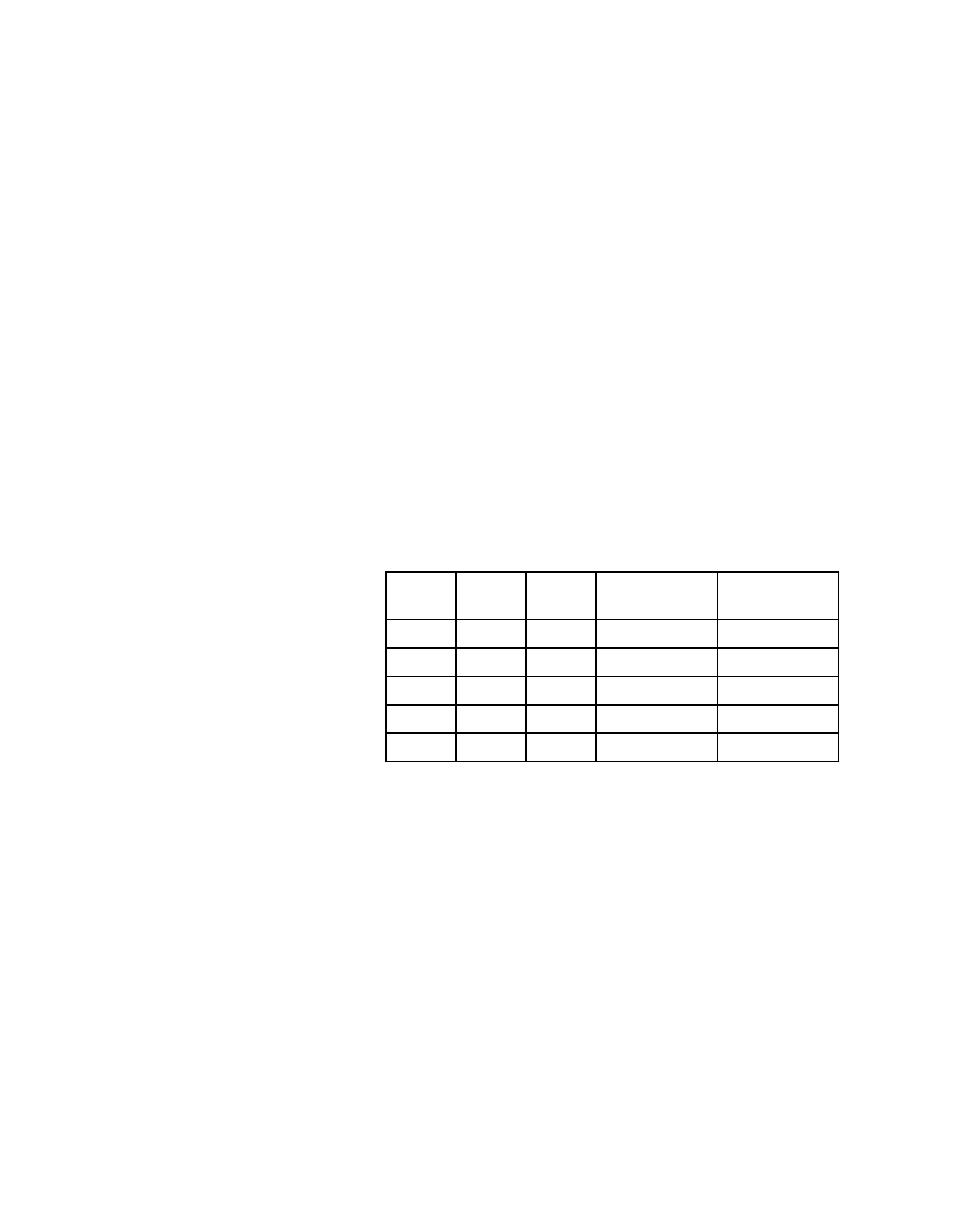
FBL2
FBL1
FBL0
DMA FIFO
Byte Lane
Pins
0
x
x
Disabled
N/A
1
0
0
0
D[7:0]
1
0
0
1
D[15:8]
1
0
1
2
D[23:16]
1
0
1
3
D[31:24]