5 pci and external memory interface timing, Pci and external memory interface timing, Lsi53c875 pci and external memory interface timing – Avago Technologies LSI8751D User Manual
Page 286
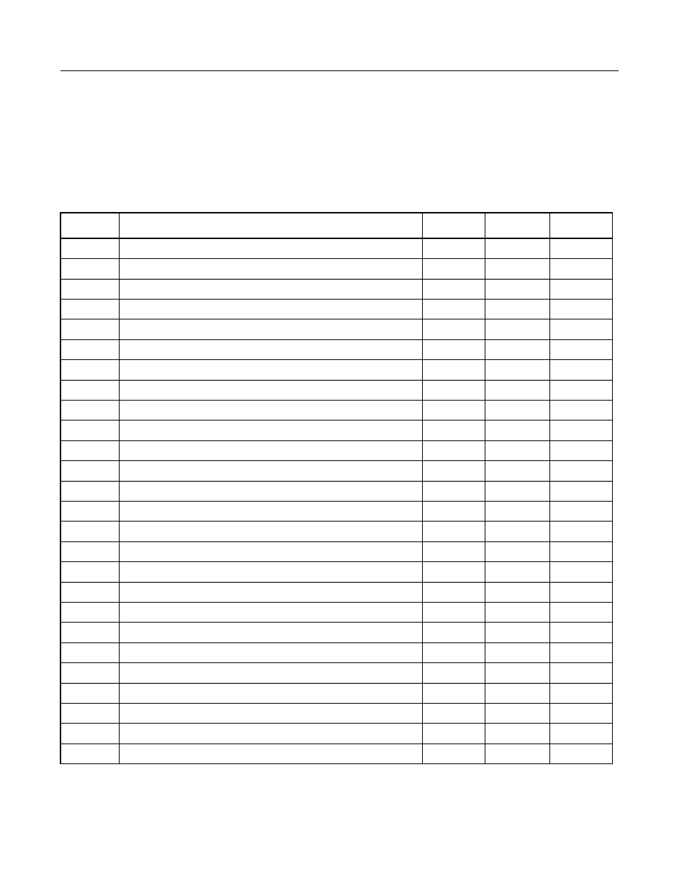
7-50
Instruction Set of the I/O Processor
7.5 PCI and External Memory Interface Timing
lists the LSI53C875 PCI and External Memory Interface timing
data.
Table 7.19
LSI53C875 PCI and External Memory Interface Timing
Symbol
Parameter
Min
Max
Unit
t
1
Shared signal input setup time
7
–
ns
t
2
Shared signal input hold time
0
–
ns
t
3
CLK to shared signal output valid
–
11
ns
t
4
Side signal input setup time
10
–
ns
t
5
Side signal input hold time
0
–
ns
t
6
CLK to side signal output valid
–
12
ns
t
7
CLK high to FETCH/ low
–
20
ns
t
8
CLK high to FETCH/ high
–
20
ns
t
9
CLK high to MASTER/ low
–
20
ns
t
10
CLK high to MASTER/ high
–
20
ns
t
11
Address setup to MAS/ high
25
–
ns
t
12
Address hold from MAS/ high
15
–
ns
t
13
MAS/ pulse width
25
–
ns
t
14f
MCE/ low to data clocked in (fast memory)
160
–
ns
t
14s
MCE/ low to data clocked in (slow memory)
220
–
ns
t
15f
Address valid to data clocked in (fast memory)
205
–
ns
t
15s
Address valid to data clocked in (slow memory)
265
–
ns
t
16f
MOE/ low to data clocked in (fast memory)
100
–
ns
t
16s
MOE/ low to data clocked in (slow memory)
160
–
ns
t
17
Data hold from address, MOE/, MCE/ change
0
–
ns
t
18
Next address out from MOE/, MCE/ high
50
–
ns
t
19
Data setup to CLK high
5
–
ns
t
20
Data setup to MWE/ low
30
–
ns
t
21
Data hold from MWE/ high
20
–
ns
t
25
MCE/ low to MWE/ low
25
–
ns
t
26
MWE/ high to MCE/ high
25
–
ns