Determining the synchronous transfer rate – Avago Technologies LSI8751D User Manual
Page 50
2-26
Functional Description
2.5.11.1 Determining the Data Transfer Rate
Synchronous data transfer rates are controlled by bits in two different
registers of the LSI53C875. Following is a brief description of the bits.
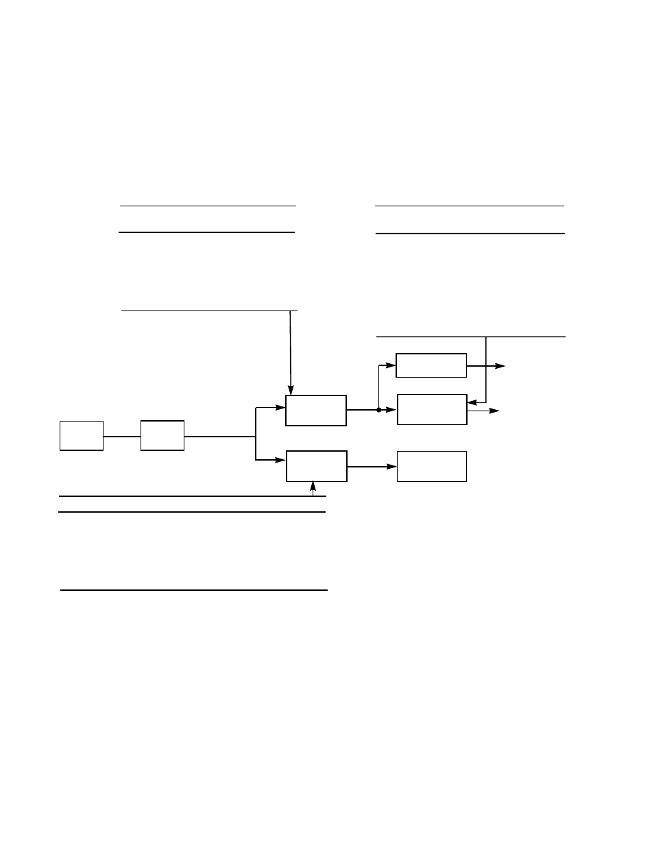
illustrates the clock division factors used in each register, and
the role of the register bits in determining the transfer rate.
Figure 2.5
Determining the Synchronous Transfer Rate
2.5.11.2
Register, Bits [6:4] (SCF[2:0])
The SCF[2:0] bits select the factor by which the frequency of SCLK is
divided before being presented to the synchronous SCSI control logic.
The output from this divider controls the rate at which data can be
received; this rate must not exceed 80 MHz. The receive rate of
synchronous SCSI data is one-fourth of the SCF divider output. For
SCLK
SCF
Divider
CCF
Divider
Synchronous
Divider
Asynchronous
SCSI Logic
Divide by 4
SCF2
SCF1
SCF0
SCF
Divisor
0
0
1
1
0
1
0
1.5
0
1
1
2
1
0
0
3
0
0
0
3
1
0
1
4
TP2
TP1
TP0
XFERP
Divisor
0
0
0
4
0
0
1
5
0
1
0
6
0
1
1
7
1
0
0
8
1
0
1
9
1
1
0
10
1
1
1
11
CCF2
CCF1
CCF0
Divisor
0
0
1
1
0
1
0
1.5
0
1
1
2
1
0
0
3
0
0
0
3
1
0
1
4
Example (8-bit SCSI bus):
SCLK = 80 MHz, SCF = 1 (
÷ 1)
, XFERP = 4 (
÷
4),
CCF = 5 (
÷
4)
This point
must not
exceed
80 MHz
Receive
Clock
Send Clock
(to SCSI Bus)
This point
must not
exceed
25 MHz
= (80
ч
1)
ч
4 = 20 Mbytes/s
SCSI receive rate = (SCLK
÷
SCF)
ч
4
= (80
ч
1)
ч
4 = 20 Mbytes/s
Clock
Doubler
SCSI send rate = (SCLK
÷
SCF)
÷
XFERP