Avago Technologies LSI8751D User Manual
Page 129
5-13
at a time, with the least significant byte on SD[7:0]/, SDP/
and the most significant byte on SD[15:8]/, SDP1/.
Command, Status, and Message phases are not affected
by this bit.
Clearing this bit will also clear the Wide SCSI Receive bit
in the
register, which
indicates the presence of a valid data byte in the
register.
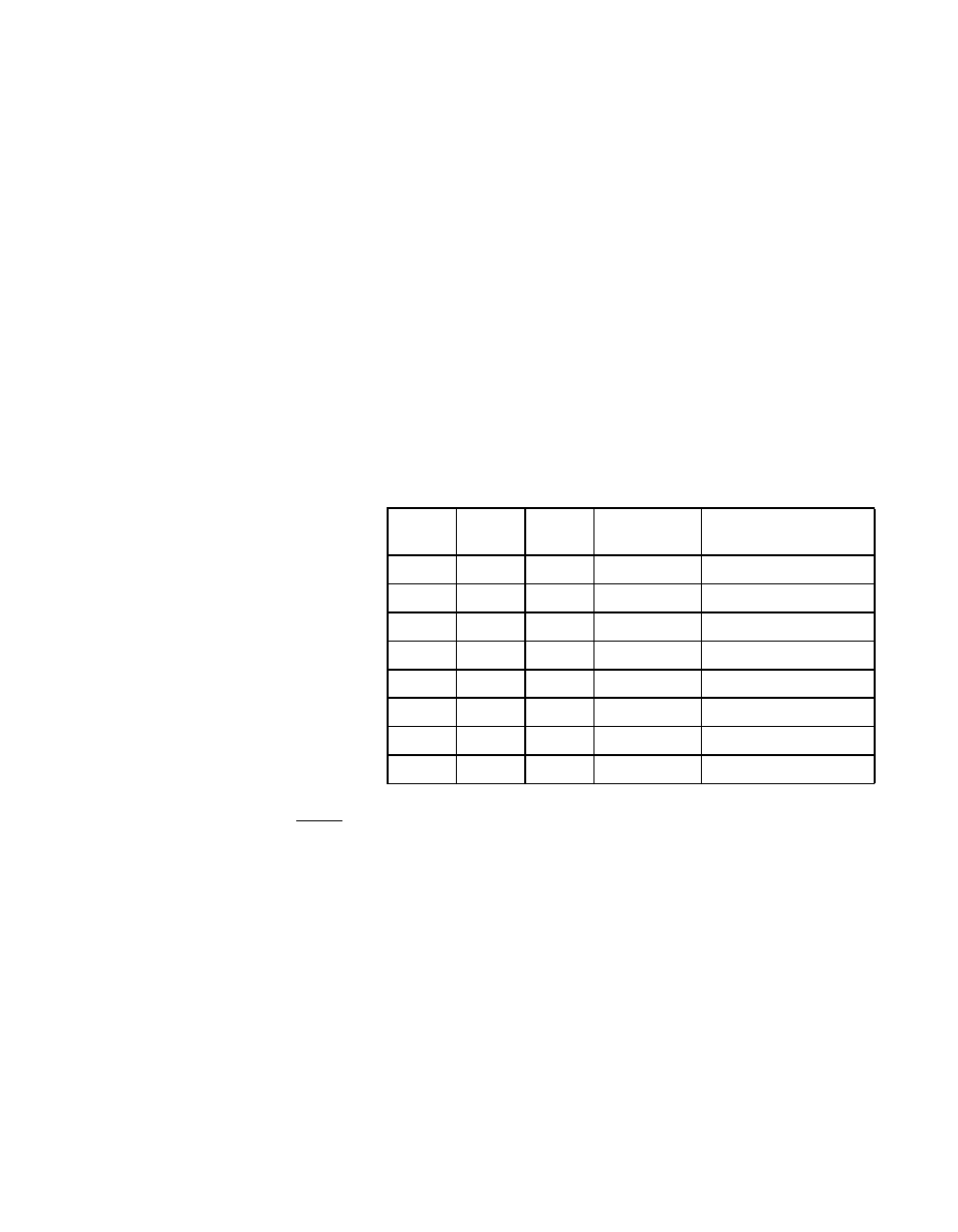
CCF[2:0]
Clock Conversion Factor
[2:0]
These bits select a factor by which the frequency of
SCLK is divided before being presented to the SCSI core.
The synchronous portion of the SCSI core can be run at
a different clock rate for fast SCSI, using the
Synchronous Clock Conversion Factor bits. The bit
encoding is displayed in the table below. All other
combinations are reserved and should never be used.
Note:
It is important that these bits be set to the proper values to
guarantee that the LSI53C875 meets the SCSI timings as
defined by the ANSI specification.
For additional information on how the synchronous
transfer rate is determined, refer to
To migrate from a Fast SCSI-2 system with a 40 MHz
clock, divide the clock by a factor of two or more to
achieve the same synchronous transfer rate in a system
with an 80 MHz clock.
SCF2
CCF2
SCF1
CCF1
SCF0
CCF0
Factor
Frequency
SCSI Clock
(MHz)
0
0
0
SCLK/3
50.01–75.0
0
0
1
SCLK/1
16.67–25.0
0
1
0
SCLK/1.5
25.01–37.5
0
1
1
SCLK/2
37.51–50.0
1
0
0
SCLK/3
50.01–75.0
1
0
1
SCLK/4
75.01–80.00
1
1
0
Reserved
–
1
1
1
Reserved
–