Figure 2-7. usb port map—10 pins, Table 2-15. psc3 functions by pin (continued), Pin drivers and mux logic 2 5 – Freescale Semiconductor MPC5200B User Manual
Page 88
Pinout Tables
MPC5200B Users Guide, Rev. 1
Freescale Semiconductor
2-43
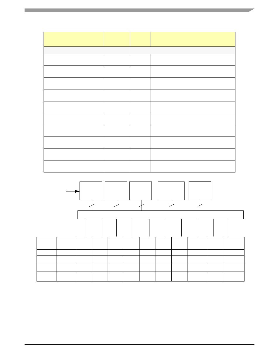
Figure 2-7. USB Port Map—10 Pins
Pin PSC3_9 Ball C04
GPIO
hi - z
GPIO_W/WAKE_UP
Simple General Purpose I/O with WAKE UP
USB2
hi - z
USB2_OVRCRNT
USB Over Current
UART3
hi - z
GPIO_W/WAKE_UP
Simple General Purpose I/O with WAKE UP
UART3e
hi - z
GPIO_W/WAKE_UP
Simple General Purpose I/O with WAKE UP
CODEC3
hi - z
GPIO_W/WAKE_UP
Simple General Purpose I/O with WAKE UP
CODEC3_w/MCLK
hi - z
GPIO_W/WAKE_UP
Simple General Purpose I/O with WAKE UP
SPI
hi - z
SPI_CLK
SPI Clock
UART3, SPI
hi - z
SPI_CLK
SPI Clock
UART3e, SPI
hi - z
SPI_CLK
SPI Clock
CODEC3, SPI
hi - z
SPI_CLK
SPI Clock
Table 2-15. PSC3 Functions by Pin (continued)
PIN / BALL NUMBER
Function
Reset
Value
Description
USB Clock
from PSC6 Port
GPIO
USB Host
RST_CFG
Pin Drivers and MUX Logic
2
5
USB_5
USB_6
USB_7
USB_8
USB_9
10
USB_0
USB_1
USB_2
USB_3
USB_4
PSC4
4
PSC5
4
Function
Port_conf
[18:19]
USB_0
USB_1
USB_2
USB_3
USB_4
USB_5
USB_6
USB_7
USB_8
USB_9
RST_CFG
---
RST_CFG6 RST_CFG7
GPIO
00
GPIO
GPIO
GPIO
GPIO
INTERRUPT
USB
01
USB1_OE USB1_TXN USB1_TXP USB1_RXD USB1_RXP USB1_RXN USB1_POR
TPWR
USB1_SPEED USB1_SUS
PEND
USB1_OVERCNT
2x UART4/5
10
GPIO
UART4_RT
S
UART4_TX
D
UART4_RXD UART4_CTS UART5_RXD UART5_TXD
UART5_RTS
UART5_CTS
INTERRUPT
NOTE:
1. If not used for USB, this port is available as a GPIO resource.
2. USB clock source can be generated internally or sourced fromUSB_CLK input.
3. Pins 3–5 are not mapped to any function other than USB.
4. RST_config bits are sampled only during Reset.
5. PSC4/5 can be used here or on the Ethernet port, but not in both places.