3 base address register overview – Freescale Semiconductor MPC5200B User Manual
Page 363
MPC5200B Users Guide, Rev. 1
10-66
Freescale Semiconductor
Application Information
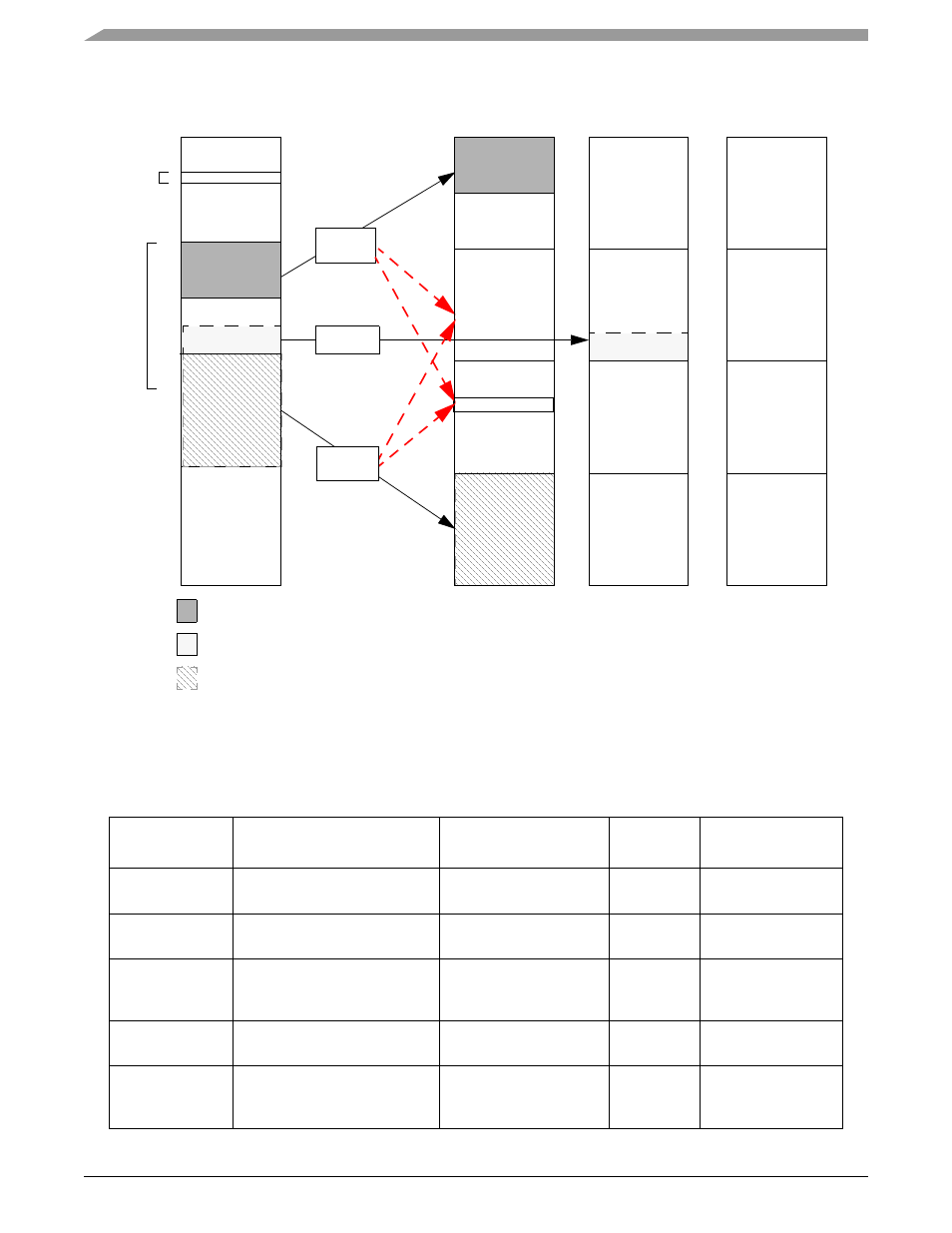
Figure 10-9. Outbound Address Map
10.6.2.1.3
Base Address Register Overview
shows the available accessibility for all PCI associated base address and translation address registers in MPC5200B.
Base Address
Register
Register Function
PCI Bus Configuration
Access
Processor
Access
Any XL bus Master
Access
BAR0
PCI Base Address Register 0
(256 Kbyte)
X
X
X
BAR1
PCI Base Address Register 1 (1
Gbyte)
X
X
X
TBATR0
Target Base Address
Translation Register 0
(256Kbyte)
X
X
TBATR1
Target Base Address
Translation Register 0 (1 Gbyte)
X
X
IMWBAR
Initiator Window
Base/Translation Address
Registers
X
X
PCI Space (Memory View)
PCI Space (IO View)
0
1G
2G
3G
4G
Window 2
Window 1
Window 0
Translation
Window 1
Translation
Associated with PCI Prefetchable Memory
Associated with PCI Non-Prefetchable Memory
MBAR
Window 2
0
1G
2G
3G
4G
0
1G
2G
3G
4G
0
1G
2G
3G
4G
PCI Space (Configuration View)
Associated with PCI I/O
Register Space
Not Recommended
MPC5200B Space
MPC5200
B mem-
MPC5200B mem-
XL Bus Initiator
Windows
Window 0
Window 0
Window 1
Not Recommended
Window 2
Translation
Window 0 Base Address = 0x40
Window 0 Address Mask = 0x1F
Window 0 Translation Address = 0x00
Window 1 Base Address = 0x70
Window 1 Address Mask = 0x0F
Window 1 Translation Address = 0x70
Window 2 Base Address = 0x80
Window 2 Address Mask = 0x3F
Window 2 Translation Address = 0xC0