1 mode register 1 (0x00)-mr1, Mode register 1 (0x00)—mr1 -5, Mode register 1 (0x00) for uart mode -5 – Freescale Semiconductor MPC5200B User Manual
Page 516: Mode register 1 (0x00)—mr1
PSC Registers—MBAR + 0x2000, 0x2200, 0x2400, 0x2600, 0x2800, 0x2C00
MPC5200B Users Guide, Rev. 1
Freescale Semiconductor
15-5
PSC module operation is controlled by writing control bytes into the appropriate registers.
15.2.1
Mode Register 1 (0x00)
—
MR1
The Mode registers control configuration. MR1 can be read or written when the Mode register pointer points to it, at reset or after a reset Mode
register pointer command using
[MISC]. After MR1 is read or written, the pointer points to
44
Infrared Control 1 (0x44)—IRCR1
8
R/W
48
Infrared Control 2 (0x48)—IRCR2
8
R/W
4C
Infrared SIR Divide Register (0x4C)—IRSDR
8
R/W
50
Infrared MIR Divide Register (0x50)—IRMDR
8
R/W
54
Infrared FIR Divide Register (0x54)—IRFDR
8
R/W
58
Rx FIFO Number of Data (0x58)—RFNUM
16
R
5C
Tx FIFO Number of Data (0x5C)—TFNUM
16
R
60
32
R/W
64
16
R/W
68
8
R/W
6E
16
R/W
72
Rx FIFO Read Pointer (0x72)—RFRPTR
16
R/W
76
Rx FIFO Write Pointer(0x76)—RFWPTR
16
R/W
7A
Rx FIFO Last Read Frame (0x7A)—RFLRFPTR
- Reserved
16
R/W
7C
Rx FIFO Last Write Frame PTR (0x7C)—RFLWFPTR
- Reserved
16
R/W
80
32
R/W
84
16
R/W
88
8
R/W
8E
16
R/W
92
Tx FIFO Read Pointer (0x92)—TFRPTR
16
R/W
96
Tx FIFO Write Pointer (0x96)—TFWPTR
16
R/W
9A
Tx FIFO Last Read Frame (0x9A)—TFLRFPTR
- Reserved
16
R/W
9C
Tx FIFO Last Write Frame PTR (0x9C)—TFLWFPTR
- Reserved
16
R/W
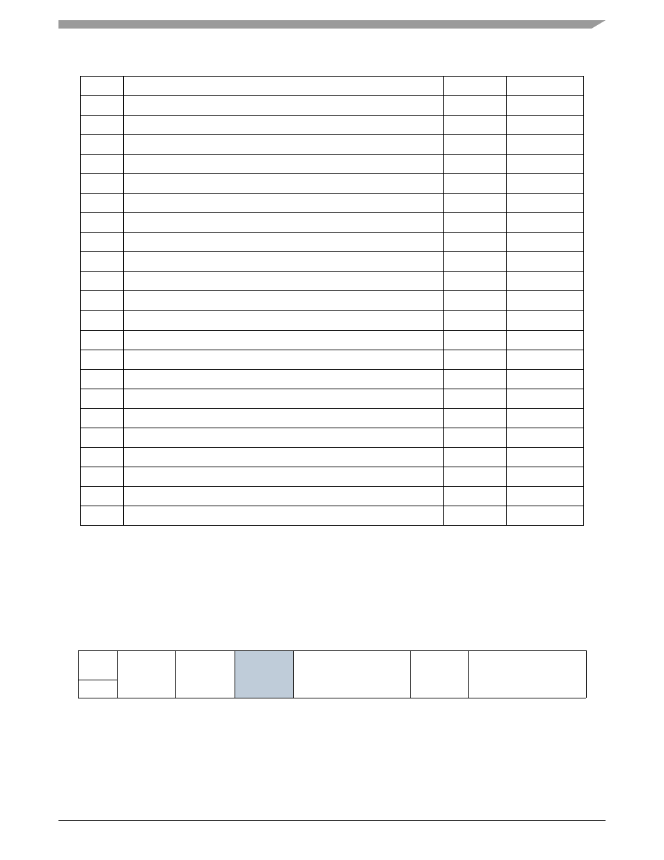
Table 15-3. Mode Register 1 (0x00) for UART Mode
msb 0
1
2
3
4
5
6
7 lsb
R
RxRTS
RxIRQ/FFUL
L
Reserved
PM
PT
B/C
W
RESET:
0
0
1
0
0
0
0
0
Table 15-2. PSC Memory Map (continued)