Freescale Semiconductor MPC5200B User Manual
Page 256
Memory Controller Registers (MBAR+0x0100:0x010C)
MPC5200B Users Guide, Rev. 1
Freescale Semiconductor
8-23
The
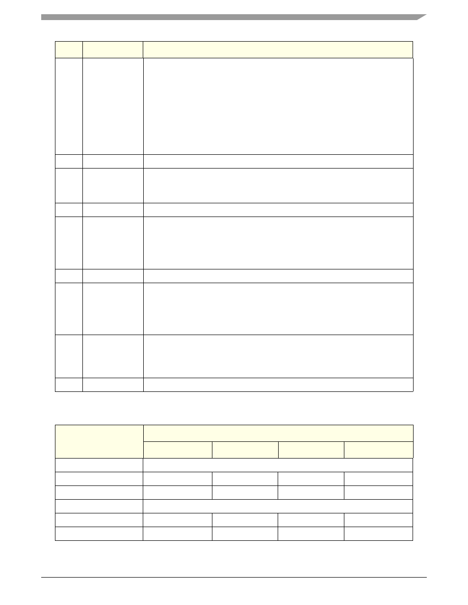
Table 8-7
indicates how the internal address bits XLA[4:7] are multiplexed internally to support higher column or row address bits.
10:15
ref_interval[0:5]
The average periodic interval at which the controller generates refresh commands to
memory; measured in increments of 64 x MEM_CLK period.
1) Multiply t
REFI
by the MEM_CLK frequency. (If the memory data sheet does not define
t
REFI
, it can be calculated by t
REFI
= t
REF
/ #rows.)
Example: Assume t
REF
= 64ms, #rows = 4K, MEM_CLK = 133MHz. Then:
t
REFI
= 64ms / 4K = 15.625
µs; 15.625µs x 133MHz = 2078.1
2) Divide the previous result by 64, rounding toward 0
2078.1 / 64 = 32.471; discard the fractional part.
3) Subtract 1 from the previous result. The new result is ref_interval.
32 - 1 = 31 = 0x1f
16:17
—
Reserved
18
mem_ps
Memory data port size.
0 32-bit data bus.
1 16-bit data bus (upper two data bytes, MEM_MDQ[31:16]).
19
—
Reserved
20:23
dqs_oe[3:0]
Each bit individually controls one MEM_MDQS output.
0 The corresponding MEM_MDQS pin is never driven, regardless of memory operation
and drive_rule. Always set to 0000 for SDR.
1 The corresponding MEM_MDQS pin can be driven, depending on memory operations
and drive_rule. DDR only.
24:28
—
Reserved
29
soft_ref
0 No operation.
1 Generate a non-periodic Auto Refresh command as soon as possible.
This is a write-only bit; always returns 0 on a read. A software requested refresh is
completely independent of the periodic refresh interval counter. Software refresh is only
possible when mode_en==1.
30
soft_pre
0 No operation.
1 Generate a Precharge All command as soon as possible.
This is a write-only bit; always returns 0 on a read. Software precharge is only possible
when mode_en==1.
31
—
Reserved
Table 8-7. High Address Usage
hi_addr
XL Bus Address Line Mapping to Column or Row Address
4
5
6
7
32-Bit Data Bus
0
CA12
CA11
CA9
CA8
1
CA11
CA9
CA8
RA12
16-Bit Data Bus
0
CA13
CA12
CA11
CA9
1
CA12
CA11
CA9
RA8
Bit
Name
Description