Bdlc rate select register -14 – Freescale Semiconductor MPC5200B User Manual
Page 693
MPC5200B Users Guide, Rev. 1
20-14
Freescale Semiconductor
Memory Map and Registers
20.7.3.6
BDLC Rate Select Register (DLCBRSR) - MBAR + 0x1309
This register determines the divider prescaler value for the mux interface clock (f
bdlc
). Only integer multiple of the 1 MHz or 1.048576 MHz
f
bdlc
are supported as input clock.
READ: any time
WRITE: write once in normal and emulation modes.
R7-R0
—
Rate Select (Bits 7-0)
These bits determine the amount by which the frequency of the system clock signal is divided to generate the MUX Interface clock (f
bdlc
)
which defines the basic timing resolution of the MUX Interface. The value programmed into these bits is dependent on the chosen system
clock frequency. See
for example rate selects for different bus frequencies. All divisor values from divide by 1 to
divide by 256 are possible, but are not shown in the tables.
NOTE
Although the maximum divider is 256, a divider which will generate a 1 MHz or 1.048576 MHz f
bdlc
must be selected in order for J1850 communications to occur.
01111
15
15
10000
16
16
10001
17
17
10010
18
18
10011
19
19
10100
20
20
10101
21
21
10110
22
22
10111
23
23
11000
24
24
11001
25
25
11010
26
26
11011
27
27
11100
28
28
11101
29
29
11110
30
30
11111
31
31
Note:
1.
The transmitter symbol timing adjustment is the same for binary and integer bus frequencies.
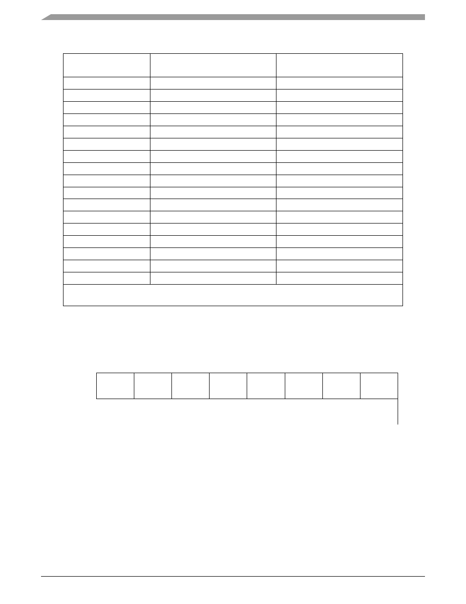
Table 20-8. BDLC Rate Select Register
msb 0
1
2
3
4
5
6
7 lsb
R
R7
R6
R5
R4
R3
R2
R1
R0
W
RESET:
0
0
0
0
0
0
0
0
Table 20-7. BARD Values vs. Transceiver Delay and Transmitter Timing Adjustment (continued)
BARD Offset Bits BO[4:0]
Corresponding Expected
Transceiver’s delays (
µ
s)
Transmitter Symbol Timing
Adjustment (
t
bdlc
)
1