Psc codec block diagram -45, Psc codec interface in slave mode -45, Figure 15-6 – Freescale Semiconductor MPC5200B User Manual
Page 561: Shows, Cdm psc
MPC5200B Users Guide, Rev. 1
15-50
Freescale Semiconductor
PSC Operation Modes
15.3.2.1
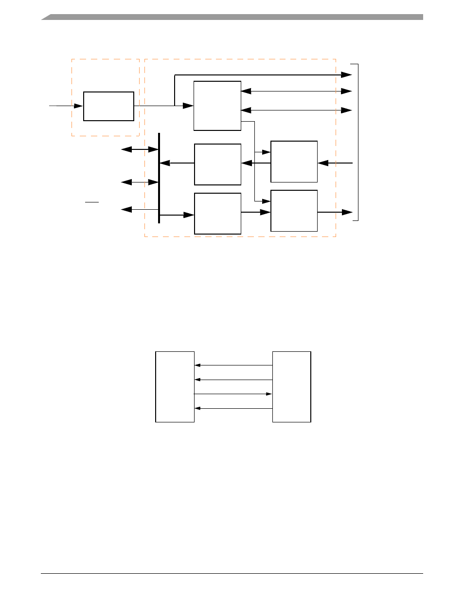
Block Diagram and Signal Definition for Codec Mode
Figure 15-6. PSC Codec Block Diagram
NOTE
Here is important difference between PSC6 and the other PSCs. To work with PSC6 in slave mode
(CODEC slave, SPI slave), the ext_48MHz_en bit in the
cdm_48mhz_fractional_divider_configuration register must be set to one. If this bit was set to zero
then the internal 48 Mhz clock generator drive the clock line. For more informations see
CDM 48MHz Fractional Divider Configuration Register—MBAR + 0x0210
Figure 15-7. PSC Codec Interface in Slave Mode
Receiver
Transmitter
Rx FIFO
Tx FIFO
Clock
Generation
Unit
RxD
TxD
BitClk
Frame
External
Interface
Signals
Mclk
IPB
Interface
CommBus
Interface
IRQ
Controller
Mclk
Mclk
Divider
f
system
CDM
PSC
BitClkDiv[0:15]+1
MclkDiv[8:0]+1
FRAME
SCLK0
SRx0
CLK
TxD
RxD
SSYNC0
STx0
external
PSC
Codec device