5 memory map / register definition, 1 module memory map, Section 19.5, memory map / register definition – Freescale Semiconductor MPC5200B User Manual
Page 642
Memory Map / Register Definition
MPC5200B Users Guide, Rev. 1
Freescale Semiconductor
19-3
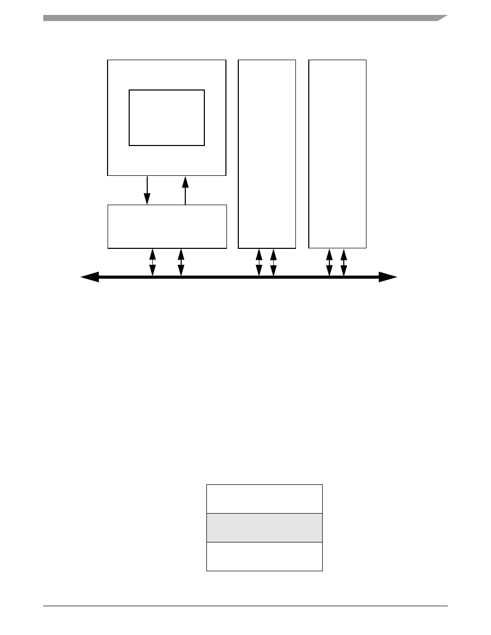
Figure 19-2. The CAN System
19.5
Memory Map / Register Definition
The MPC5200B contains 2 independent MSCAN Controller :
•
MSCAN1 = MBAR + 0x0900
•
MSCAN2 = MBAR + 0x0980
19.5.1
Module Memory Map
give an overview on all registers and their individual bits in the MSCAN memory map. The register address results
from the addition of base address and address offset. The base address is determined at the MPC5200B MCU level. The address offset is
defined at the module level.
The MSCAN occupies 64 bytes in the memory space. The base address of the MSCAN module is determined at the MPC5200B MCU level
when the MCU is defined. The register decode map is fixed and begins at the first address of the module address offset.
Table 19-1. MSCAN Register Organization
Address
Offset
$__00
CONTROL REGISTERS
12 BYTES
$__15
$__18
RESERVED
2 BYTES
$__19
$__1C
ERROR COUNTERS
2 BYTES
$__1D
CAN Bus
CAN Controller
(MSCAN)
Transceiver
CAN node 1
CAN node 2
CAN node n
CAN_L
CAN_H
MCU
TXCAN
RXCAN