Psc ac97 block diagram -56, Psc signal description for ac97mode -56 – Freescale Semiconductor MPC5200B User Manual
Page 573
MPC5200B Users Guide, Rev. 1
15-62
Freescale Semiconductor
PSC Operation Modes
15.3.3.1
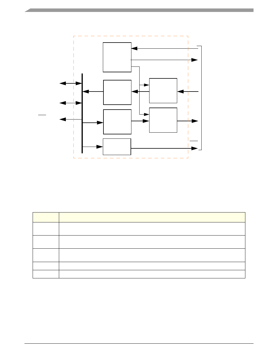
Block Diagram and Signal Definition for AC97 Mode
Figure 15-14. PSC AC97 Block Diagram
shows the simplified PSC Block Diagram for AC97 mode. The BitClk is an input from the external Codec. The PSC divide
BitClk by 256 to generate a Frame pulse (Sync) that is high for 16 BitClk cycles. The PSC can only work as AC97 controller, it’s means that
the PSC receive the BitClk from the external AC97 codec and provide the associated Frame signal. In AC97 mode the Clock and Frame
relations are fixed, therefore the
register and the
[GenClk] bit are not used. The table below shows the Pin definition for the AC97
mode and the
shows an AC97 interface. An MPC5200 general-purpose I/O (GPIO) is used as a reset to the external AC97 device.
Table 15-87. PSC Signal Description for AC97 Mode
Signal
Description
Sdata_out
Transmitter Serial Data Output—Data is shifted out on TxD on the rising edge of the clock signal.
Transfers must be specified as msb first.
Sdata_in
Receiver Serial Data Input—Data received on RxD is sampled on the falling edge of the clock signal.
Transfers must be specified as msb first.
Sync
In AC97 mode Sync is the frame sync, or start-of-frame (SOF), output to the external AC97 Controller.
In this mode the AC97 BitClk, which is input on CLK, is divided by 256 to generate the Sync.
BitClk
BitClk— In AC97 mode CLK must be driven by the serial bit-clock from the external AC97 Controller.
Res
Reset signal to the external AC97 device
Receiver
Transmitter
Rx FIFO
Tx FIFO
Clock
Generation
Unit
Sdata_in
Sdata_out
BitClk
Sync
External
Interface
Signals
IPB
Interface
CommBus
Interface
IRQ
Controller
PSC
Res
Reset
Logic