3 processor bus (xlb ) clock domain, 4 sdram memory controller clock domain, Processor bus (xlb ) clock domain – Freescale Semiconductor MPC5200B User Manual
Page 140: Sdram memory controller clock domain
MPC5200B Clock Domains
MPC5200B Users Guide, Rev. 1
Freescale Semiconductor
5-7
NOTE
The XLB CLOCK frequency and the ppc_pll_cfg[0:4] must be chosen such that resulting CORE
CLOCK frequency and PLL (f
VCOcore
) frequency do not exceed their respective maximium or
minimum operating frequencies. Refer to
and MPC5200B Hareware Specification.
5.3.3
Processor Bus (XLB ) Clock Domain
The XLB clock (xlb_clk) is the fundamental MPC5200B clock frequency. The following operate at this frequency:
•
The internal processor address/data bus
•
The internal SDRAM Controller
•
External SDRAM
All functional blocks that interface to the XLB must operate at this frequency, or have a section of logic that operates at this frequency.
5.3.4
SDRAM Memory Controller Clock Domain
The Memory Controller uses the clocks shown in
.
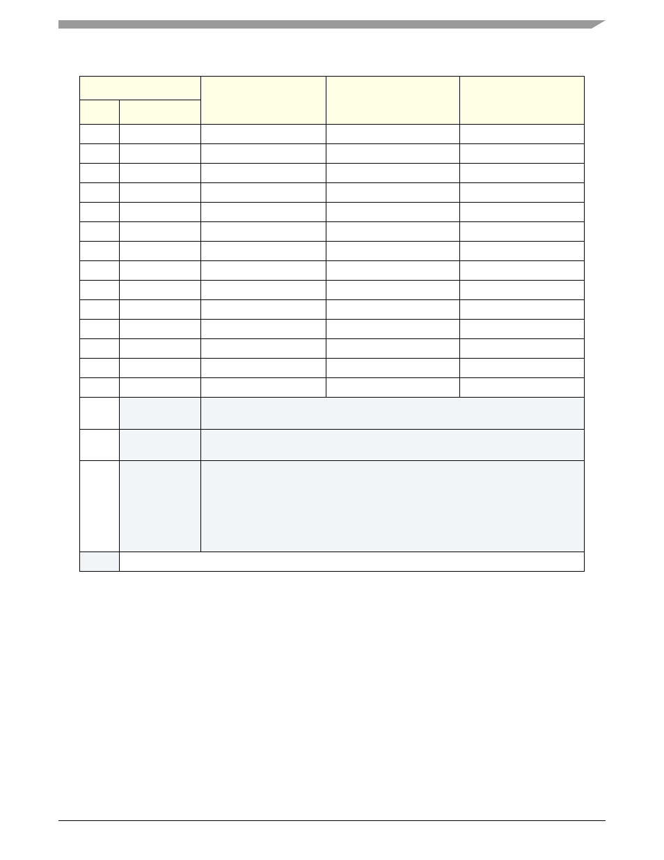
0x08
01000
1:3
1:2
1:6
0x09
01001
1:5.5
1:2
1:11
0x0A
01010
1:4
1:2
1:8
0x0B
01011
1:5
1:2
1:10
0x0C
01100
—
—
—
0x0D
01101
1:6
1:2
1:12
0x0E
01110
1:3.5
1:2
1:7
0x10
10000
1:3
1:4
1:12
0x11
10001
1:2.5
1:4
1:10
0x12
10010
1:6.5
1:2
1:13
0x14
10100
1:7
1:2
1:14
0x16
10110
1:7.5
1:2
1:15
0x18
11000
—
—
—
0x1C
11100
1:8
1:2
1:16
0x03
0x13
00011
10011
PLL off/bypassed
xlb_clk clocks core directly, 1x bus-to-core
0x0F
0x1F
01111
11111
PLL off, no core clocking occurs.
0x15
0x17
0x19
0x1A
0x1B
0x1D
0x1E
10101
10111
11001
11010
11011
11101
11110
Reserved, should not be used.
Note: Shading implies same mode can be configured with ppc_pll_cfg[0]=0
Table 5-6. e300 Core APLL Configuration Options (continued)
ppc_pll_cfg
Bus:Core Ratio
(XLB : CORE CLOCK)
Core:VCO Ratio
(CORE CLOCK: f
VCOcore
)
Bus:VCO Ratio
(XLB : f
VCOcore)
hex
[0:1:2:3:4]