11 ata ultra dma timing 5 register-mbar + 0x3a28, 12 ata share count register-mbar + 0x3a2c, 2 ata fifo registers-mbar + 0x3a00 – Freescale Semiconductor MPC5200B User Manual
Page 373: Section 11.3.2, Section 11.3.2, ata fifo registers—mbar + 0x3a00, Ata ultra dma timing 5 register, Ata_shre_cnt
MPC5200B Users Guide, Rev. 1
11-8
Freescale Semiconductor
ATA Register Interface
11.3.1.11
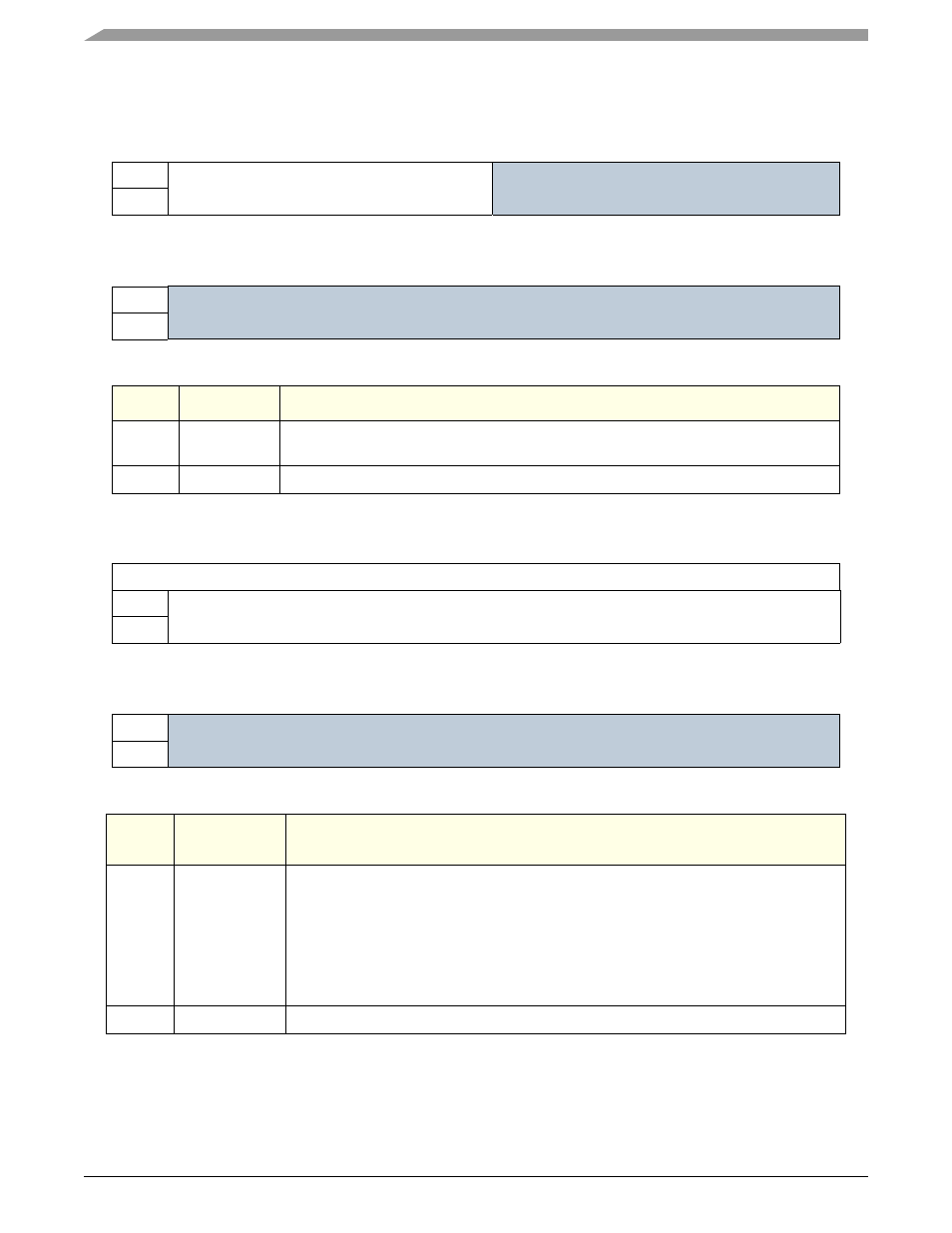
ATA Ultra DMA Timing 5 Register—MBAR + 0x3A28
11.3.1.12
ATA Share Count Register—MBAR + 0x3A2C
11.3.2
ATA FIFO Registers—MBAR + 0x3A00
ATA uses a single FIFO that changes direction based on the Rx/Tx mode. Software controls direction change and flushes FIFO before
changing directions. FIFO memory is 512Bytes (Four 8 x 128 memories).
Table 11-11. ATA Ultra DMA Timing 5 Register
msb 0
1
2
3
4
5
6
7
8
9
10
11
12
13
14
15
R
udma_tzah
Reserved
W
RESET:
0
0
0
0
0
0
0
0
0
0
0
0
0
0
0
0
16
17
18
19
20
21
22
23
24
25
26
27
28
29
30
31 lsb
R
Reserved
W
RESET:
0
0
0
0
0
0
0
0
0
0
0
0
0
0
0
0
Bits
Name
Description
0:7
udma_tzah
Minimum delay time required for output drivers to assert or negate from release state.
Count value is based on system clock operating frequency.
8:31
—
Reserved
Table 11-12.
ata_shre_cnt
msb0
1
2
3
3
5
6
7
8
9
10
11
12
13
14
15
R
ata_share_cnt
W
RESET:
0
0
0
0
0
0
0
0
1
0
0
0
0
0
0
0
16
17
18
19
20
21
22
23
24
25
26
27
28
29
30
31 lsb
R
Reserved
W
RESET:
0
0
0
0
0
0
0
0
0
0
0
0
0
0
0
0
Bits
Name
Description
0:15
ata_share_cnt
This 16-bit value controls the length of the “time slot” assigned to ATA transactions when
PCI arbiter provides a grant to the ATA device. This is in IPB clocks. The arbiter will
maintain the grant to ATA for (at least) the ata_share_cnt value. When this value has
expired, ATA may be interrupted (paused) by the arbiter, to service other pending requests
for the AD bus.
Default value at reset is 128
Note: The maximal allowed setting is 0xFFFE.
16:31
—
Reserved