1 ata register addressing, 2 drive interrupt, 3 sector addressing – Freescale Semiconductor MPC5200B User Manual
Page 393
MPC5200B Users Guide, Rev. 1
11-28
Freescale Semiconductor
ATA Bus Background
11.7.3.1
ATA Register Addressing
The address used to reference an ATA drive register. This is the actual address (CS[1]FX, CS[3]FX, DA[2:0]) present on the physical ATA
interface.
gives details.
11.7.3.2
Drive Interrupt
A pending drive interrupt is cleared by the following actions:
•
Read of status (not the alternate status) register
•
Write to command register
11.7.3.3
Sector Addressing
Sector addressing is the address used to reference data on the drive. It is the address used by the low-level drivers to access a particular piece
of data and to place it into one or more ATA registers as part of a command block. To understand the data addressing, it is necessary to
understand the physical organization of data in a drive, as presented in
. Each drive contains a number of disks, each with one or
two heads (one head per surface). Each disk is divided into concentric tracks that are then divided into a number of sectors. A sector is the
smallest unit of data that can be written or read by a drive. The collections of tracks that can be accessed by the heads at a single position is
called a cylinder. Therefore, a sector can be uniquely identified by a sector number, a head number and a cylinder number. From this
addressing scheme there are two ways to address an individual sector: physical addressing and logical block addressing, which are described
in the next two sections.
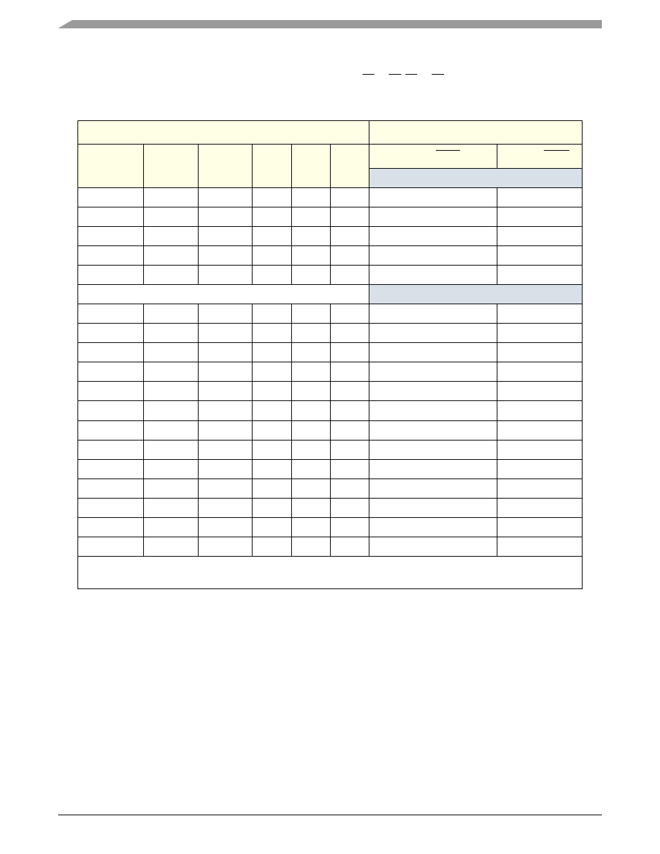
Table 11-37. ATA Register Address/Chip Select Decoding
Address
Function
System
Address
CS[1]FX
CS[3]FX
DA[2]
DA[1]
DA[0]
READ (DIOR)
WRITE (DIOW)
Control Block Registers
—
1
1
x
x
x
Data bus high impedance
Not used
03F0–03F3
1
0
0
x
x
Data bus high impedance
Not used
03F4–03F5
1
0
1
0
x
Data bus high impedance
Not used
03F6
1
0
1
1
0
Alternate status
Device control
03F7
1
0
1
1
1
Obsolete
Not used
Command Block Registers
01F0
0
1
0
0
0
Data
Data
01F1
0
1
0
0
1
Error register
Features
01F2
0
1
0
1
0
Sector count
Sector count
01F3
0
1
0
1
1
Sector number
Sector number
01F3
0
1
0
1
1
LBA bits 0–7
1
LBA bits 0–7
1
01F4
0
1
1
0
0
Cylinder low
Cylinder low
01F4
0
1
1
0
0
LBA bits 8–15
1
LBA bits 8–15
1
01F5
0
1
1
0
1
Cylinder high
Cylinder high
01F5
0
1
1
0
1
LBA bits 16–23
1
LBA bits 16–23
1
01F6
0
1
1
1
0
Drive/head
Drive/head
01F6
0
1
1
1
0
LBA bits 24–27
1
LBA bits 24–27
1
01F7
0
1
1
1
1
Status
Command
—
0
0
x
x
x
Invalid address
Invalid address
Note:
1.
LBA mode register mapping—system addresses are for a single channel, accommodating two drives only.