2 ata rx / tx fifo status register-mbar + 0x3a40, 1 ata rx/tx fifo data word register—mbar + 0x3a3c – Freescale Semiconductor MPC5200B User Manual
Page 374
ATA Register Interface
MPC5200B Users Guide, Rev. 1
Freescale Semiconductor
11-9
ATA FIFO is controlled by 32-bit registers. These registers are located at an offset from MBAR of 0x3a00. Register addresses are relative to
this offset. Therefore, the actual register address is:
MBAR + 0x3A00 + register address
Hyperlinks to the ATA FIFO registers are provided below:
11.3.2.1
ATA Rx/Tx FIFO Data Word Register—MBAR + 0x3A3C
11.3.2.2
ATA Rx/Tx FIFO Status Register—MBAR + 0x3A40
•
ATA Rx/Tx FIFO Data Word Register
(0x3A3C)
•
(0x3A48)
•
ATA Rx/Tx FIFO Status Register
(0x3A40)
•
ATA Rx/Tx FIFO Read Pointer Register
(0x3A4C)
•
ATA Rx/Tx FIFO Control Register
(0x3A44)
•
ATA Rx/Tx FIFO Write Pointer Register
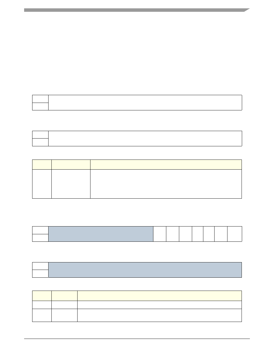
Table 11-13. ATA Rx/Tx FIFO Data Word Register
msb 0
1
2
3
4
5
6
7
8
9
10
11
12
13
14
15
R
FIFO_Data_Word
W
RESET:
0
0
0
0
0
0
0
0
0
0
0
0
0
0
0
0
16
17
18
19
20
21
22
23
24
25
26
27
28
29
30
31 lsb
R
FIFO_Data_Word
W
RESET:
0
0
0
0
0
0
0
0
0
0
0
0
0
0
0
0
Bits
Name
Description
0:31
FIFO_Data_Word
The FIFO data port. Reading from this location “pops” data from the FIFO, writing
“pushes” data into the FIFO. During normal operation the BestComm Controller
pushes data here.
Note: ONLY full long-word access is allowed. If all byte enables are not asserted
when accessing this location, a FIFO error flag is generated.
Table 11-14. ATA Rx/Tx FIFO Status Register
msb 0
1
2
3
4
5
6
7
8
9
10
11
12
13
14
15
R
Reserved
Err
UF
OF
Full
HI
LO
Emty
W
RESET:
0
0
0
0
0
0
0
0
0
0
0
0
0
0
0
0
16
17
18
19
20
21
22
23
24
25
26
27
28
29
30
31 lsb
R
Reserved
W
RESET:
0
0
0
0
0
0
0
0
0
0
0
0
0
0
0
0
Bits
Name
Description
0:8
—
Reserved
9
Err
Error—flag bit is essentially the logical "OR" of other flag bits and can be polled for detection
of any FIFO error. After clearing the offending condition, writing 1 to this bit clears flag.