Table 9-7 – Freescale Semiconductor MPC5200B User Manual
Page 278
Programmer’s Model
MPC5200B Users Guide, Rev. 1
Freescale Semiconductor
9-13
9.7.1.1
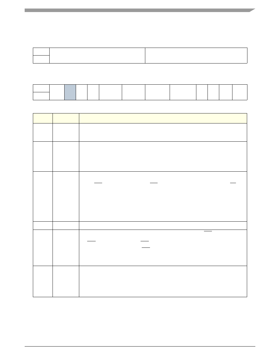
Chip Select 0/Boot Configuration Register—MBAR + 0x0300
Table 9-7. Chip Select 0/Boot Configuration Register
msb 0
1
2
3
4
5
6
7
8
9
10
11
12
13
14
15
R
WaitP
WaitX
W
RESET:
0
0
0
0
0
0
0
0
cfg
cfg
cfg
cfg
cfg
cfg
cfg
cfg
16
17
18
19
20
21
22
23
24
25
26
27
28
29
30
31 lsb
R
MX
Rsvd
AA
CE
AS
DS
Bank
WTyp
WS
RS
WO
RO
W
RESET:
cfg
1
1
1
cfg
cfg
cfg
cfg
0
0
0
0
0
0
0
1
Bits
Name
Description
0:7
WaitP
Number of wait states to insert. Can be applied as a prescale to WaitX or used by itself, as
specified by WTyp bits below. Wait states control how many PCI clocks the corresponding
CS pin remains active.
8:15
WaitX
Base number of wait states to insert, or combined with WaitP as specified by WTyp bits
below.
cfg operation—If rstcfg[11] (on pad_eth_03) is zero then 4 wait states are in effect, else 48
wait states are in effect. Wait States equals the number of PCI clocks from CS assertion to
when data must be valid from boot device.
16
MX
MX bit specifies whether a transaction operates as multiplexed or non-multiplexed. A
multiplexed transaction presents address and data in different tenures. During the address
tenure, ALE is asserted. At the end of ALE, AD bus is switched to data tenure and CSx pin
is asserted.
0 = Non-multiplexed
1 = Multiplexed
cfg operation—If rstcfg[14] on pad_eth_06 is low, boot operation is non-multiplexed (single
tenure), else boot operation is multiplexed (dual tenure).
17
—
Reserved
18
AA
ACK Active—multiplexed transactions only. This bit defines whether ALK input is active or
not. If AA is 1, programmed wait states can be overridden when/if the external device drives
the ACK input low. If AA is 0, the ACK input is ignored.
Wait states are still in effect. If no ACK is received, cycle terminates at end of wait state
period.
Note: Bit must be set to 0, to use ACK as burst indication signal during a burst transaction.
19
CE
An individual Enable bit—allows CS operation for the corresponding CS pin. CE must be high
to allow operation. Chip Select Control Register ME bit must also be high, except when
CS[0] is used for boot ROM.
1 = Enable
0 = Disabled, register writes can occur but no external access is generated.