Figure 4–7 – Altera IP Compiler for PCI Express User Manual
Page 68
4–10
Chapter 4: IP Core Architecture
Transaction Layer
IP Compiler for PCI Express User Guide
August 2014
Altera Corporation
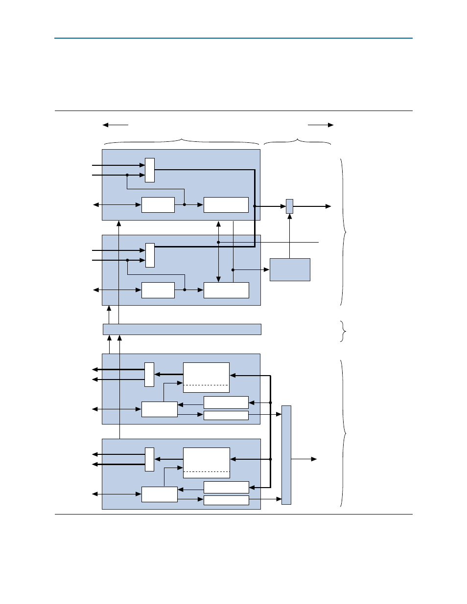
5. The receive sequencing and reordering block shuffles the order of waiting
transaction layer packets as needed, fetches the address of the priority transaction
layer packet from the transaction layer packet FIFO block, and initiates the transfer
of the transaction layer packet to the application layer.
Figure 4–7. Architecture of the Transaction Layer: Dedicated Receive Buffer per Virtual Channel
Tx1 Data
Tx1 Descriptor
Tx1 Control
Virtual Channel 1
Tx0 Data
Tx0 Descriptor
Tx0 Control
Virtual Channel 0
Rx Flow
Control Credits
Tx Transaction Layer
Packet Description
& Data
Virtual Channel
Arbitration & Tx
Sequencing
Rx0 Data
Rx0 Descriptor
Rx0 Control
& Status
Virtual Channel 0
Rx1 Data
Rx1 Descriptor
Rx1 Control
& Status
Type 0 Configuration Space
Receive Buffer
Tx Flow
Control Credits
Rx Transaction
Layer Packet
Interface Established per Virtual Channel
Interface Established per Component
Transmit
Data Path
Configuration
Space
Receive
Data Path
Towards Data Link Layer
Towards Application Layer
Tx0 Request
Sequencing
Flow Control
Check & Reordering
Tx1 Request
Sequencing
Flow Control
Check & Reordering
Rx0 Sequencing
& Reordering
Posted & Completion
Non-Posted
Rx1 Sequencing
& Reordering
Virtual Channel 1
Flow Control Update
Transaction Layer
Packet FIFO
Receive Buffer
Posted & Completion
Non-Posted
Flow Control Update
Transaction Layer
Packet FIFO