Altera IP Compiler for PCI Express User Manual
Page 118
5–32
Chapter 5: IP Core Interfaces
Avalon-ST Interface
IP Compiler for PCI Express User Guide
August 2014
Altera Corporation
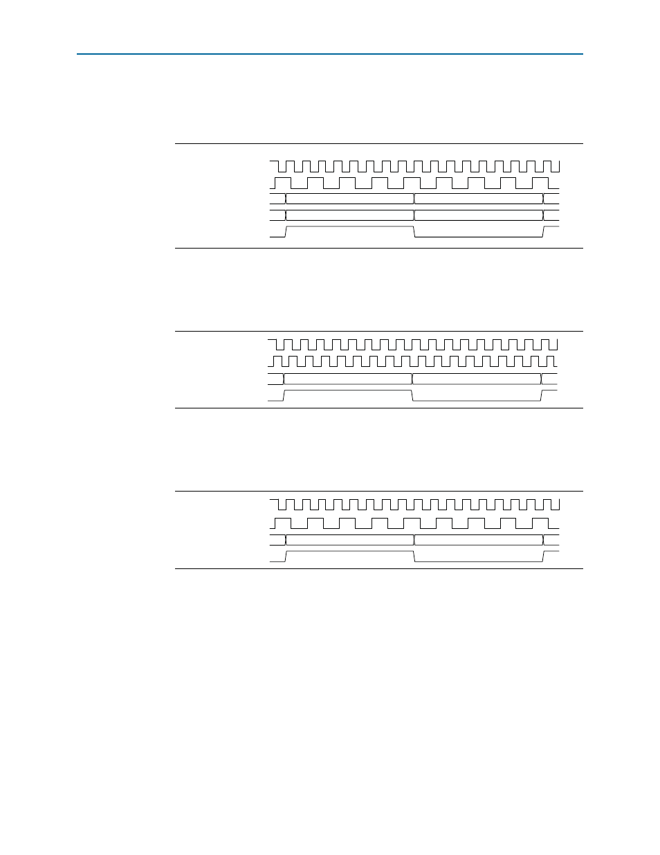
illustrates the timing of the tl_cfg_ctl interface for the Arria II GX,
Cyclone IV GX, HardCopy IV, and Stratix IV GX devices when using a 128-bit
interface.
illustrates the timing of the tl_cfg_sts interface for the Arria II GX,
Cyclone IV GX, HardCopy IV, and Stratix IV GX devices when using a 64-bit
interface.
illustrates the timing of the tl_cfg_sts interface for the Arria II GX,
Cyclone IV GX, HardCopy IV, and Stratix IV GX devices when using a 128-bit
interface.
In the example design created with the IP Compiler for PCI Express, you can use a
Verilog HDL module or VHDL entity included in the altpcierd_tl_cfg_sample.v or
altpcierd_tl_cfg_sample.vhd
file, respectively, to sample the configuration space
signals. In this module or entity the tl_cfg_ctl_wr and tl_cfg_sts_wr signals are
registered twice and then the edges of the delayed signals are used to enable sampling
of the tl_cfg_ctl and tl_cfg_sts busses.
Because the hard IP core_clk is much earlier than the pld_clk, the Quartus II
software tries to add delay to the signals to avoid hold time violations. This delay is
only necessary for the tl_cfg_ctl_wr and tl_cfg_sts_wr signals. You can place
multicycle setup and hold constraints of three cycles on them to avoid timing issues if
the logic shown in
is used. The multicycle setup and hold
contraints are automatically included in the
with the hard IP variation. In some cases, depending on the exact device, speed grade,
Figure 5–29. tl_cfg_ctl Timing (Hard IP Implementation)
Figure 5–30. tl_cfg_sts Timing (Hard IP Implementation)
Figure 5–31. tl_cfg_sts Timing (Hard IP Implementation)
core_clk
tl_cfg_ctl[31:0]
tl_cfg_add[3:0]
tl_cfg_ctl_wr
data0
data1
addr0
addr1
pld_clk 128-bit mode
core_clk
pld_clk 64-bit mode
tl_cfg_sts[52:0]
tl_cfg_sts_wr
data0
data1
core_clk
pld_clk 128-bit mode
tl_cfg_sts[52:0]
tl_cfg_sts_wr
data0
data1